Nanoimprint resin stamper

a technology of resin stamping and nano-printing, which is applied in the field of nano-print resin stamping and nano-structure transfer apparatus, can solve the problems of inability to reuse once damaged and high cost of molds, and achieve the effects of reducing the occurrence of foreign matter, reducing the cost of mold damage, and reducing the cost of mold repair

Inactive Publication Date: 2011-09-13
HITACHI HIGH-TECH CORP
View PDF11 Cites 16 Cited by
  • Summary
  • Abstract
  • Description
  • Claims
  • Application Information

AI Technical Summary

Benefits of technology

[0012]According to this invention, the vulnerable and difficult-to-strip rigid mold is replaced by a less vulnerable and easy-to-strip flexible mold, with the result that the throughput of the UV nanoimprint process is markedly improved. The mold is expensive and cannot be reused once damaged; on the other hand, given the mold, as many resin stampers as are desired can be replicated at low cost. In addition, since the support member is larger in size than the intermediate layer and the patterned resin layer, the resin stamper can be transported and aligned automatically by holding the support member having mechanical strength. Furthermore, since the highly flexible intermediate layer is capable of elastic deformation, the effects of any foreign matter or protrusions on the transfer substrate can be mitigated.
[0014]According to this invention, the planarizing film helps improve the planar precision of the intermediate layer and, hence, the planar precision of the patterned resin layer.
[0016]According to this invention, the presence of the release treated film markedly enhances the strippability of the resin stamper from a transfer substrate.
[0021]Thus, according to one aspect of the present invention, the vulnerable and difficult-to-strip rigid mold is replaced by a less vulnerable and easy-to-strip flexible mold, with the result that the throughput of the UV nanoimprint process is markedly improved. The rigid mold fabricated with an e-beam lithographic apparatus is expensive and cannot be reused once damaged; on the other hand, given the mold, as many resin stampers as are desired can be replicated at low cost. In addition, since the support member is larger in size than the intermediate layer and the patterned resin layer, the resin stamper can be transported and aligned automatically by holding the support member having mechanical strength. Furthermore, since the highly flexible intermediate layer is capable of elastic deformation, the effects of any foreign matter or protrusions on the transfer substrate can be mitigated.
[0022]According to the other aspect of the present invention, since the patterned resin layer of the resin stamper is smaller in size than the transfer substrate, a specified UV nanoimprint operation can be performed on the transfer substrate by means of the resin stamper while the transfer substrate is being clamped by the clamp mechanism and, after the imprinting operation, the resin stamper can be automatically stripped from the transfer substrate by descending the stage as the transfer substrate remains clamped by the clamp mechanism. Consequently, problems that often occurred with the conventional nanostructure transfer apparatus, such as the damage to the rigid mold and the occurrence of foreign matter, can be entirely eliminated.

Problems solved by technology

The mold is expensive and cannot be reused once damaged; on the other hand, given the mold, as many resin stampers as are desired can be replicated at low cost.

Method used


Image

  • Nanoimprint resin stamper
  • Nanoimprint resin stamper
  • Nanoimprint resin stamper

Examples


example 1

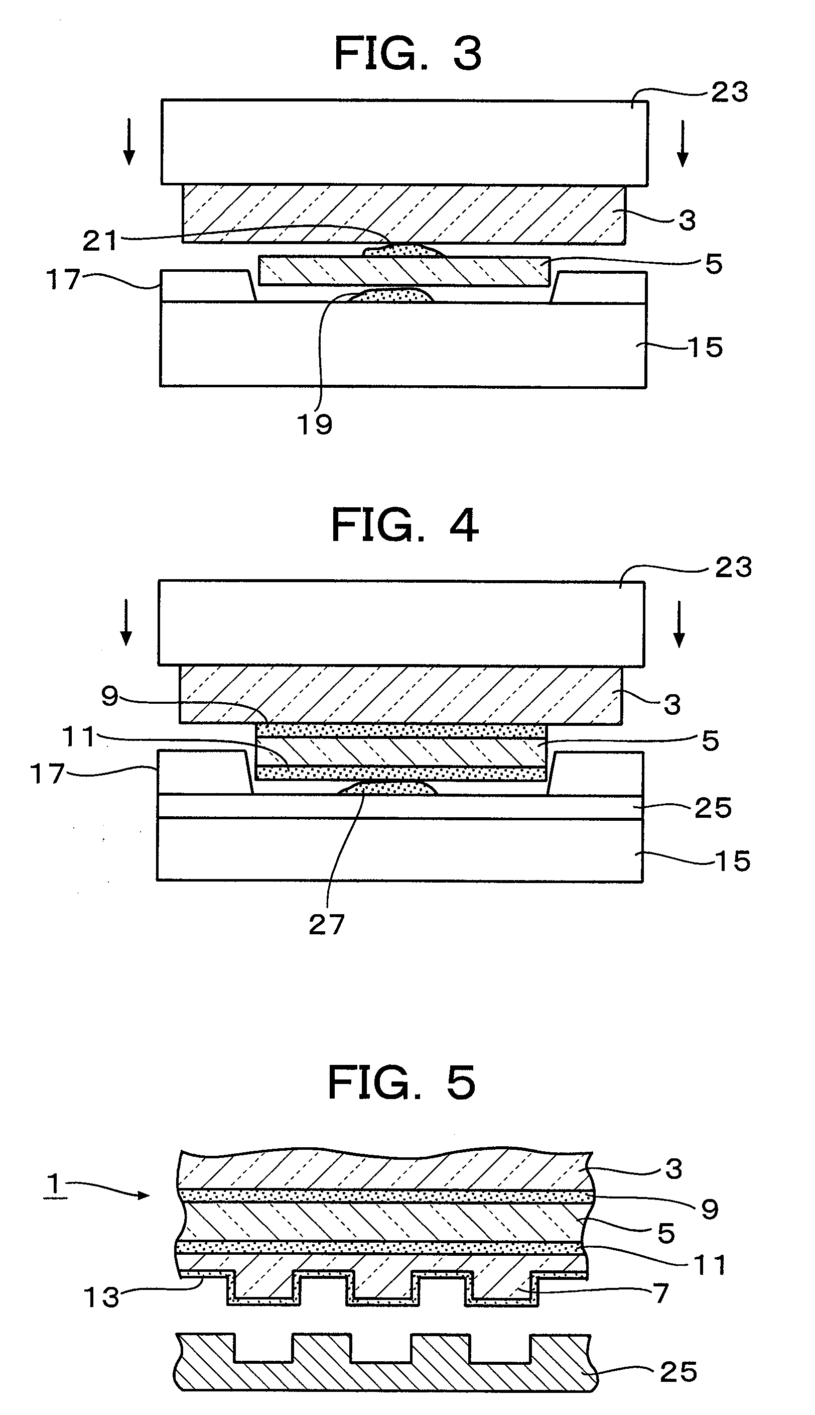
[0053]This example describes an operation that uses the nanoimprint resin stamper 1 of FIG. 5 to transfer a nano-scale pattern from the patterned resin layer 7 to the transfer substrate 41 by means of the nanostructure transfer apparatus of FIG. 6.

[0054]In the nanostructure transfer apparatus 28, a placement table 45 having a curved surface on one side is placed on top of a vertically movable stainless steel stage 43. The placement table 45 was formed of optical glass having a diameter of 100 mm, a thickness of 20 mm, and a curvature radius R of 10.38 m. A cushion layer 47 made of silicone rubber measuring 40 mm on each side with a thickness of 8 mm was provided over the curved surface of the placement table 45; a PET sheet with alignment marks that measured 100 mm in diameter and 0.1 mm thick was interposed between the cushion layer 47 and the placement table 45. The silicone rubber of which the cushion layer 47 was made was more flexible than the optical glass of which the placeme...


PUM

PropertyMeasurementUnit
thicknessaaaaaaaaaa
thickaaaaaaaaaa
thicknessaaaaaaaaaa

Abstract

A resin stamper is provided that is intended for use in an optical transfer-based nanostructure transfer apparatus and which is capable of automatic transport and alignment. The resin stamper includes a support member made of a light transmitting material and having mechanical strength, an intermediate layer also made of a light transmitting material, and a patterned resin layer which is also made of a light transmitting material. The support member is larger in size than the intermediate layer and the patterned resin layer. The intermediate layer is more flexible than the patterned resin layer. Also, the patterned resin layer has a pattern of high and low areas formed in a surface thereof that is the obverse of the pattern of high and low areas in a mold.

Description

FIELD OF THE INVENTION[0001]The present invention relates to a nanoimprint resin stamper and a nanostructure transfer apparatus using the stamper. More particularly, the present invention relates to a nanoimprint resin stamper that has sufficient mechanical strength to be capable of providing automatic transport and alignment while exhibiting a high level of handling properties; the invention also relates to a nanostructure transfer apparatus having a mechanism that enables the stamper to be easily stripped from a transfer substrate after the transfer of a nanostructure.BACKGROUND OF THE INVENTION[0002]With remarkable advances in the performance of computers and other information equipment, the volume of information that is handled by users has been constantly increasing and is now measured in gigabytes as a unit. Under these circumstances, there exists an ever-growing demand for semiconductor devices such as information storage / reproduce equipment and memories that are capable of r...

Claims


Application Information

Patent Timeline
Patent Type & Authority Patents(United States)
IPC IPC(8): B29C59/00B29B13/08
CPCB29C33/424B29C35/0888B29C37/0053B82Y10/00B82Y40/00G03F7/0002B29C2035/0827B29C2059/023
Inventor KOMORIYA, SUSUMUMORI, KYOICHISHIZAWA, NORITAKEYAMASAKI, TAKANORIHATOGAI, TETSUHIROTSUSHIMA, KOJI
Owner HITACHI HIGH-TECH CORP
Why Eureka
Try Eureka