Memory system and method of accessing a semiconductor memory device

a memory system and memory technology, applied in the field of memory system and a method of accessing a semiconductor memory device, can solve problems such as loose storage data of volatile memory devices

Active Publication Date: 2011-09-27
SAMSUNG ELECTRONICS CO LTD
View PDF55 Cites 88 Cited by
  • Summary
  • Abstract
  • Description
  • Claims
  • Application Information

AI Technical Summary

Benefits of technology

[0446]Therefore, in the embodiment of the present invention, the first programming method aforementioned is adopted thereto when not requiring high reliability, while the second programming method described later is adopted thereto when requiring high reliability. Adopting the second programming method described later, the LSB data is not lost even when there is a program fail while programming the MSB. As a result, the nonvolatile memory device is improved in reliability.

Problems solved by technology

Volatile memory devices loose stored data when power supply is interrupted.

Method used


Image

  • Memory system and method of accessing a semiconductor memory device
  • Memory system and method of accessing a semiconductor memory device
  • Memory system and method of accessing a semiconductor memory device

Examples


embodiment 1

Flash Memory System Performing Multi-Thread Function

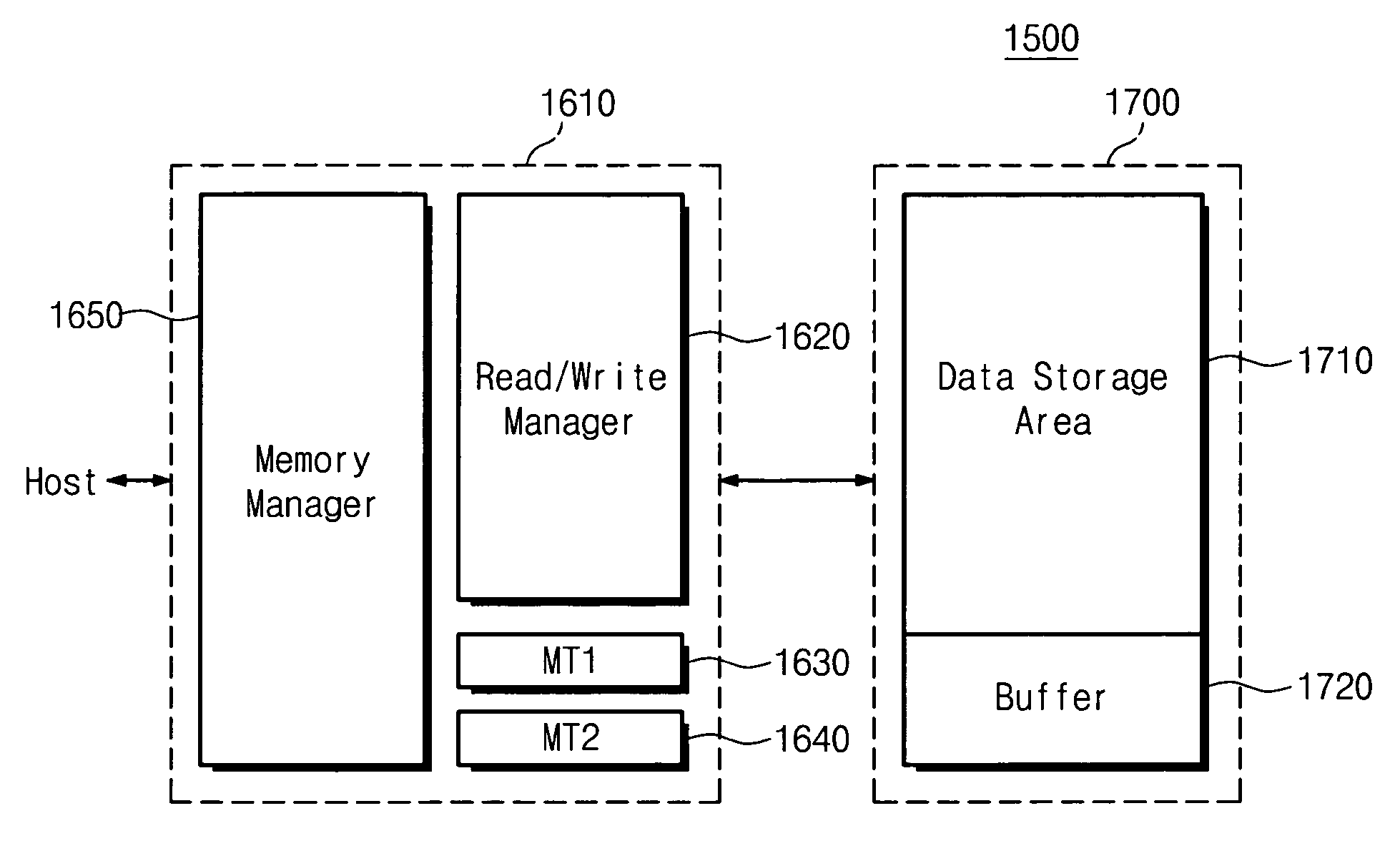
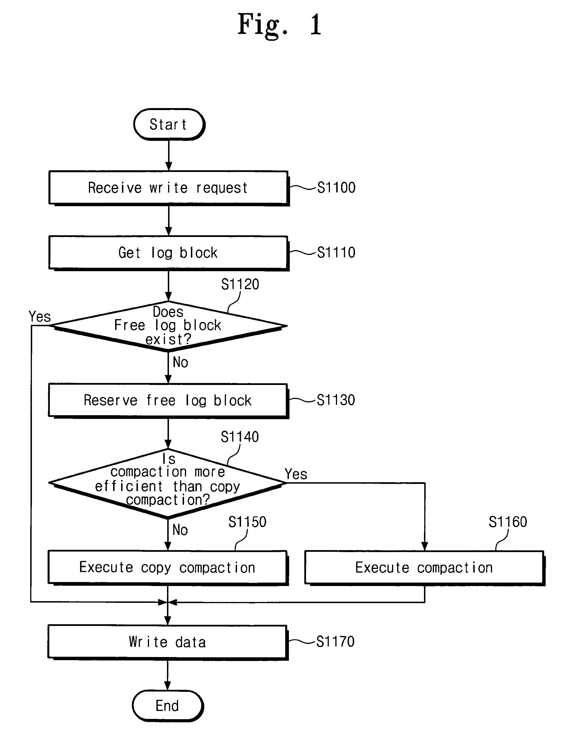
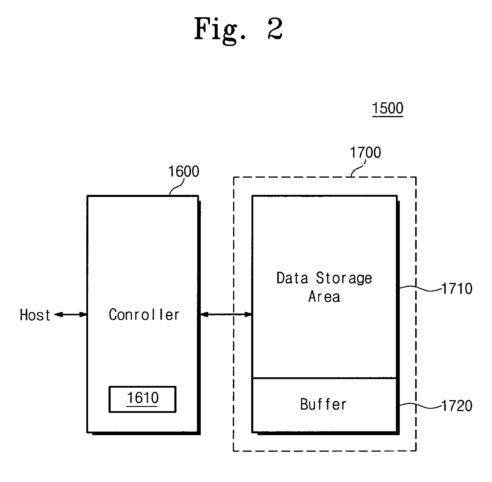
[0125]A flash memory device has erase-before-write characteristics. That is, to store data in the flash memory device, a corresponding storage space should be erased in advance. In the flash memory device, a unit of a write operation differs from that of an erase operation. The unit of the write operation is a page, whereas the unit of the erase operation is a block in the flash memory device. The number of erasing times of the flash memory device is restricted to about a hundred thousand. Because of such a characteristic of the flash memory device, additional operations besides the write operation are executed during the write operation of the flash memory device. For example, a garbage collection and a wear leveling operation may be additionally performed during the write operation of the flash memory device.

[0126]As described above, the number of erasing times is restricted to a hundred thousand. Therefore, although an erase req...

embodiment 2

Flash Memory System Having Free Page

[0224]Recently, portable electric devices such as a digital camera, an MP3 player, a mobile phone, a personal digital assistant (PDA), etc. are extensively used. Flash memories are commonly used in those portable electric devices. The reason is that flash memories are non-volatile memory devices having characteristics such as lower power consumption and high integration.

[0225]Unlike hard disks capable of overwriting data, the flash memories cannot overwrite data. That is, if flash memories try to overwrite data, existing data must be erased first. This is called erase-before-write. Before writing data, flash memories must return to an initial state or an erase state.

[0226]An erase operation of flash memories usually takes relatively longer time than a write operation. Additionally, because an erase unit of flash memories is a block, which is larger than a write unit, this may cause flash memories to erase a portion that may be unnecessary for a wr...

embodiment 3

Flash Memory System Using Microcode

[0316]A memory controller is designed using Hard-wired Logic to control all of the instruction sequences of a flash memory, in a way to enhance its performance. The memory controller designed with the Hard-wired Logic is complicated, has low extension ability, and is difficult to manage a plurality of flash memory effectively.

[0317]On the other hand, one way to increase extension ability of the memory controller is to control all of the instruction sequences of the flash memory via firmware. The designing of the memory controller according to this method may be easily done but this provides low capability. Therefore, ways to solve disadvantages of the above described two methods are required. In other words, a flash memory controller capable of extending easily with a high capability is in demand. Also, single-product memory, for example, the NAND flash memory is controlled by a CPU of a host. Products, for example, an SD card and MMC card include ...


PUM


Abstract

One embodiment of a nonvolatile memory device includes a memory cell array including a plurality of multi-level cells, and a control unit configured to determine a characteristic of data to be stored in the memory cell array. The control unit is configured to select one of plural multi-bit programming methods based on the determination. Data is stored in the memory cell array according to the selected multi-bit programming method, and at least one of the plural multi-bit programming methods maintains least significant bit data when there is a program fail of most significant bit data.

Description

CROSS-REFERENCE TO RELATED APPLICATIONS[0001]This U.S. non-provisional patent application claims priority under 35 U.S.C. §119 of Korean Patent Application Nos. 10-2008-55637 filed on Jun. 13, 2008, 10-2008-55641 filed on Jun. 13, 2008, 10-2008-55639 filed on Jun. 13, 2008, 10-2008-55642 filed on Jun. 13, 2008, 10-2008-55643 filed on Jun. 13, 2008, 10-2008-56871 filed on Jun. 17, 2008 and 10-2008-61001 filed on Jun. 26, 2008 the entire contents of which are incorporated herein by reference. This U.S. non-provisional patent application also claims priority under 35 U.S.C. §119 of U.S. Provisional Application Nos. 61 / 061,335 filed on Jun. 13, 2008, 61 / 129,241 filed on Jun. 13, 2008, 61 / 129,242 filed on Jun. 13, 2008, 61 / 129,249 filed on Jun. 13, 2008, 61 / 129,248 filed on Jun. 13, 2008, 61 / 073,632 filed on Jun. 18, 2008 and 61 / 129,600 filed on Jul. 8, 2008.BACKGROUND[0002]1. Technical Field[0003]The present invention disclosed herein relates to a semiconductor memory device, and more p...

Claims


Application Information

Patent Timeline
Patent Type & Authority Patents(United States)
IPC IPC(8): G11C16/04
CPCG11C11/5628G11C16/3418G11C16/3431G11C16/0483G06F12/0246G06F2212/7201G11C11/5642Y02B60/1225G11C29/00G11C2211/5621G06F2212/7203Y02D10/00
Inventor LEE, JAESOOROH, KANGHOCHO, WONHEESHIM, HOJUNCHOI, YOUNGJOONHEO, JAEHOONSONG, JE-HYUCKCHO, SEUNG-DUKKIM, SEONTAEKOH, MOONWOOKPARK, JONG TAECHEON, WONMOONPARK, CHANIKLEE, YANG-SUP
Owner SAMSUNG ELECTRONICS CO LTD
Why Eureka
Try Eureka