Controlled ESR decoupling capacitor

a capacitor and esr technology, applied in the field of capacitors, can solve the problems of generating unacceptable voltage spikes, needing to reduce inductance becomes a serious limitation, and no one design generally addresses all the problems, and achieves the effect of increasing esr

Active Publication Date: 2011-10-25
KYOCERA AVX COMPONENTS CORP
View PDF19 Cites 19 Cited by
  • Summary
  • Abstract
  • Description
  • Claims
  • Application Information

AI Technical Summary

Benefits of technology

[0018]Another positive aspect of this type of device is that capacitors may be produced in accordance with the present technology resulting in relatively small devices that allow for distributed placement of the devices over a circuit board.
[0025]In other variations of the foregoing exemplary embodiment, such first conductive termination layer material and such second conductive termination layer material may be configured so as to form a gap therebetween along a portion of such at least one edge of both such first and second electrode layers, whereby such current path includes a current loop area formed from such first conductive termination layer through such plurality of first electrode layers and plurality of second electrode layers to such second conductive termination layer which cooperates with an associated circuit board for forming respective current cancellation pathways, for lowering equivalent series inductance of such component. In such exemplary arrangement, preferably such terminal layer material spacing is minimized at such gap so as to provide reduction in equivalent series inductance of such component as such gap is reduced.
[0029]In certain present exemplary embodiments, a present multilayer electronic component may further comprise at least a second extended length tab connection extending respectively from each of such conductive layer main electrode area to at least one edge of its respective insulative layer first surface, so as provide dual access to each respective conductive layer so as to provide relatively reduced equivalent inductance of such component.
[0032]Yet another present exemplary embodiment relates to a multilayer land grid feedthrough vertically-oriented ceramic capacitor for mounting on a multilayer printed circuit board, for effective filtering capabilities for signal level lines and decoupling of power level lines or circuit planes, for providing controlled equivalent series resistance, and for providing low equivalent series inductance by employing current canceling techniques. Such present exemplary combination may further include a plurality of first electrode layers, each first electrode layer comprising a first insulative layer having first and second surfaces thereof bounded by four edges and a first conductive layer covering a portion of such first surface of such first insulative layer and having a main electrode area and at least one extended length tab connection extending from such first conductive layer main electrode area to at least one edge of such first insulative layer first surface; a plurality of second electrode layers alternately stacked with such plurality of first electrode layers and comprising mirror images thereof, each second electrode layer comprising a second insulative layer having first and second surfaces thereof bounded by four edges and a second conductive layer covering a portion of such first surface of such second insulative layer and having a main electrode area and at least one extended length tab connection extending from such second conductive layer main electrode area to at least one edge of such second insulative layer first surface; first conductive termination layer material covering portions of such first electrode layers and electrically connecting such first conductive layer of each of such plurality of first electrode layers; and second conductive termination layer material covering portions of such second insulative layer and electrically connecting such second conductive layer of each of such plurality of second electrode layers. In such exemplary embodiment, preferably such at least one extended length tab connections of such respective first and second conductive layers are selectively configured so as to selectively establish the effective length of respective paths to such respective conductive layers, whereby a current path is formed from such first conductive termination layer through such plurality of first electrode layers and plurality of second electrode layers to such second conductive termination layer which cooperates with an associated circuit board for forming respective current pathways having controlled equivalent series resistance for such component; such first conductive termination layer material and such second conductive termination layer material are configured so as to form a gap therebetween along a portion of such at least one edge of both such first and second electrode layers, whereby such current path includes a current loop area formed from such first conductive termination layer through such plurality of first electrode layers and plurality of second electrode layers to such second conductive termination layer which cooperates with an associated circuit board for forming respective current cancellation pathways, for lowering equivalent series inductance of such component; and terminal layer material spacing is minimized at such gap so as to provide reduction in equivalent series inductance of such component as such gap is reduced.

Problems solved by technology

As switching speeds increase and pulse rise times decrease in electronic circuit applications, the need to reduce inductance becomes a serious limitation for improved system performance.
Even the decoupling capacitors, which act as a local energy source, can generate unacceptable voltage spikes, as reflected by the calculation of V=L (di / dt).
While various aspects and alternative features are known in the field of multilayer electronic components and related methods for manufacture, no one design has emerged that generally addresses all of the issues as discussed herein.

Method used


Image

  • Controlled ESR decoupling capacitor
  • Controlled ESR decoupling capacitor
  • Controlled ESR decoupling capacitor

Examples


first embodiment

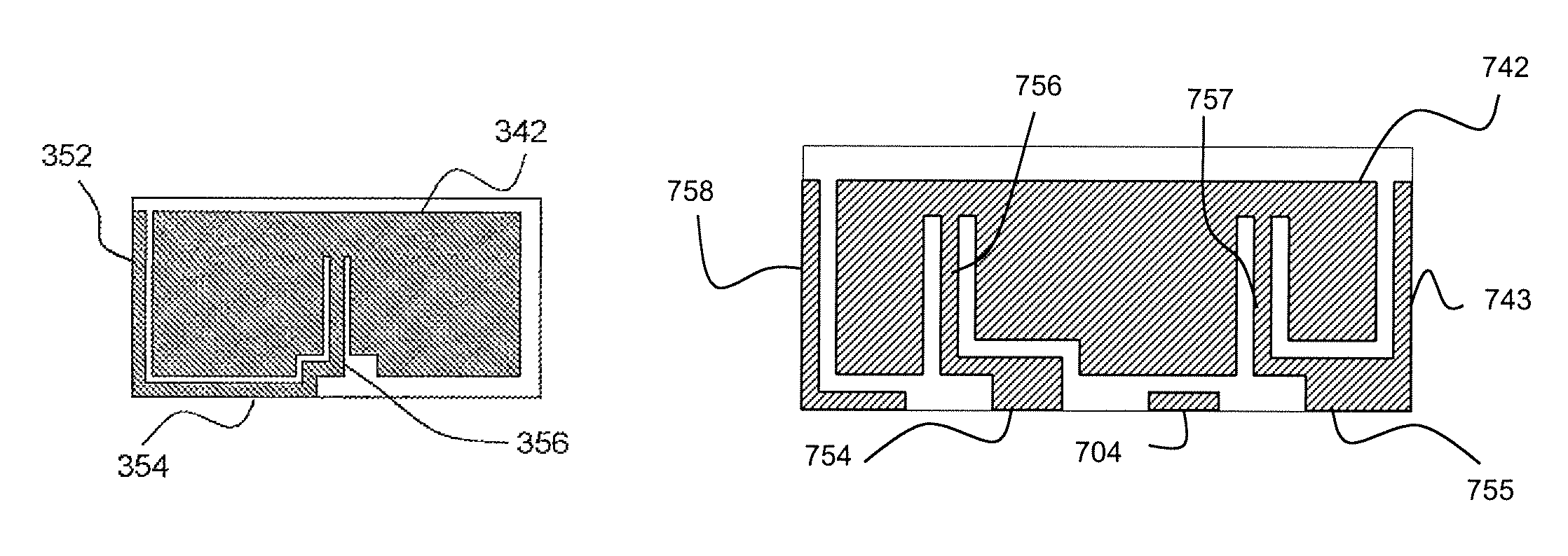
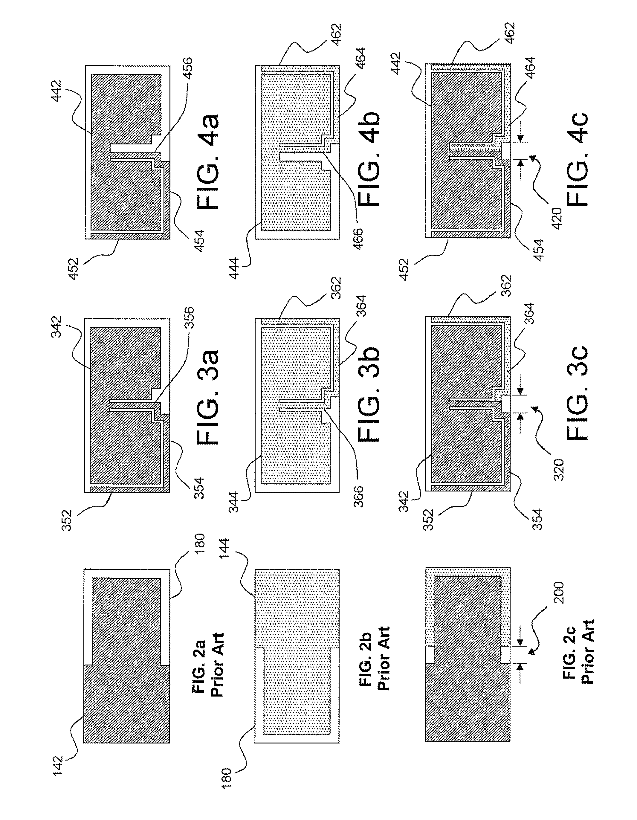
[0056]With reference to FIGS. 3a, 3b, and 3c there is illustrated the present technology wherein controlled Equivalent Series Resistance (ESR) is provided by adding path length to the active electrodes. With reference to FIGS. 3a and 3b it will be appreciated that there has been illustrated a pair of electrodes 342, 344 that are substantial mirror images of each other. Each electrode 342, 344 has substantially the same overall area as in the prior configurations illustrated in FIGS. 2a and 2b corresponding to electrodes 142, 144, respectively, but each include features that provide increased Equivalent Series Resistance (ESR).

[0057]More specifically, as will be noticed in FIG. 3a, side contact portion 352, bottom contact portion 354 and a portion of the central area 356 of electrode 342 have been separated from the main electrode area so that an extended conductive path is created thereby providing increased path length and thus increased ESR for a capacitor constructed in accordanc...

second embodiment

[0059]With reference to FIGS. 4a, 4b, and 4c there is illustrated the present technology wherein controlled Equivalent Series Resistance (ESR) is provided by adding path length to the active electrodes. With reference to FIGS. 4a and 4b it will be appreciated that there has been illustrated a pair of electrodes 442, 444 that are substantial mirror images of each other. Each electrode 442, 444 has substantially the same overall area as in the prior configurations illustrated in FIGS. 3a and 3b corresponding to electrodes 342, 344, respectively, and each include features that provide increased Equivalent Series Resistance (ESR).

[0060]More specifically, as will be noticed in FIG. 4a, side contact portion 452, bottom contact portion 454 and a portion of the central area 456 of electrode 442 have been separated from the main electrode area so that an extended conductive path is created thereby providing increased ESR for a capacitor constructed in accordance with this second exemplary em...


PUM

PropertyMeasurementUnit
areaaaaaaaaaaa
lengthaaaaaaaaaa
conductiveaaaaaaaaaa

Abstract

Disclosed are apparatus and methodology for providing controlled equivalent series resistance (ESR) decoupling capacitor designs having broad applicability to signal and power filtering technologies. Such capacitor designs provide characteristics for use in decoupling applications involving both signal level and power level environments. Controlled equivalent series resistance (ESR) is provided by providing extended length tab connections to active electrode layers within the device.

Description

PRIORITY CLAIM[0001]This application claims the benefit of previously filed U.S. Provisional Patent Application entitled “CONTROLLED ESR DECOUPLING CAPACITOR,” assigned U.S. Ser. No. 60 / 934,397, filed Jun. 13, 2007, and which is incorporated herein by reference for all purposes.FIELD OF THE INVENTION[0002]The present subject mater relates to capacitors. More particularly, the present subject matter relates to vertically oriented, multi-layer ceramic capacitor structures having broad applicability to signal and power filtering technologies.BACKGROUND OF THE INVENTION[0003]The present subject matter generally concerns improved component design for decoupling capacitors that generally results in devices characterized by relatively low cost, low inductance and controllable Equivalent Series Resistance (ESR).[0004]As switching speeds increase and pulse rise times decrease in electronic circuit applications, the need to reduce inductance becomes a serious limitation for improved system pe...

Claims


Application Information

Patent Timeline
Patent Type & Authority Patents(United States)
IPC IPC(8): H01G4/005H01G4/228H01G4/06
CPCH01G2/06H01G4/232H01G4/35H01G4/30Y10T29/435H05K1/0231H01G4/12
Inventor RITTER, ANDREW P.BEROLINI, MARIANNEVANALSTINE, KIMBERLY L.
Owner KYOCERA AVX COMPONENTS CORP
Why Eureka
Try Eureka