Semiconductor module, portable device and method for manufacturing semiconductor module
a semiconductor module and portable device technology, applied in the field of semiconductor modules, can solve the problems of increasing the power consumption of lsi chips with the associated increase in performance and functionality, increasing the need for radiation of extra heat away from the csp, and increasing so as to suppress the reducing of reliability and increase the heat radiation of the semiconductor module
- Summary
- Abstract
- Description
- Claims
- Application Information
AI Technical Summary
Benefits of technology
Problems solved by technology
Method used
Image
Examples
first embodiment
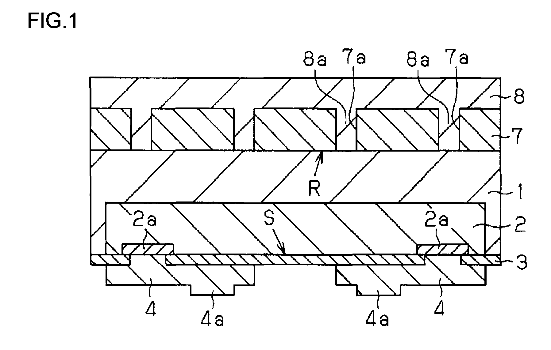
[0039]FIG. 1 is a schematic cross-sectional view of a semiconductor module according to a first embodiment of the present invention. The semiconductor module according to the first embodiment will be described with reference to FIG. 1.
[0040]A semiconductor substrate 1 is, for example, a p-silicon substrate, which has a surface S (lower surface) on which a circuit element 2, such as a predetermined electrical circuit, is formed by a technique well-known to those skilled in the art and on which electrodes 2a of the circuit element 2 are formed (circumferentially). A protective film 3 is formed on all regions of the surface of the semiconductor substrate 1 except the electrodes 2a. A re-wiring pattern 4 connected to exposed faces of the electrodes 2a and electrodes 4a which are integrally provided with the re-wiring pattern 4 are formed to ensure that the pitch of the electrodes 2a is sufficiently large. Note that the semiconductor substrate 1, the circuit element 2, the surface S, and...
second embodiment
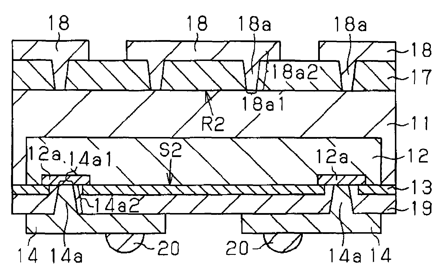
[0059]FIG. 5 is a schematic cross-sectional view of a semiconductor module according to a second embodiment of the present invention. The semiconductor module according to the second embodiment will be described with reference to FIG. 5.
[0060]A semiconductor substrate 11 is, for example, a p-silicon substrate, which has a surface S2 (lower surface) on which a circuit element 12, such as a predetermined electrical circuit, is formed by a technique well-known to those skilled in the art and on which electrodes 12a of the circuit element 12 are formed (circumferentially). A protective film 13 is formed on all regions of the surface of the semiconductor substrate 11 except the electrodes 12a. Note that the semiconductor substrate 11, the circuit element 12, and the surface S2 are examples of the “semiconductor substrate,” the “circuit element,” and the “first principal surface” of the present invention, respectively.
[0061]An insulating layer 17 is formed on a rear surface R2 (upper surf...
third embodiment
[0093]FIG. 9 is a schematic cross-sectional view of a semiconductor module according to a third embodiment of the present invention. The third embodiment differs from the second embodiment in that parts of the projections 18a are embedded in the rear surface R2 (upper surface) of the semiconductor substrate 11. The other configuration is the same as that of the second embodiment.
[0094]The configuration in which the projections 18a are embedded is achieved by forming recesses 22 in advance in regions to be connected with the projections 18a by photolithography and etching techniques, on the rear surface R2 (upper surface) of the semiconductor wafer (semiconductor substrate 11) prepared as shown in FIG. 7A. The recesses 22 are tapered suitable for portions in which the projections 18a are embedded. The recesses 22 each have a depth D of, for example, approximately 20 μm, and the projections 18a are formed higher accordingly.
[0095]The semiconductor module and the manufacturing method t...
PUM
 Abstract
Description
Claims
Application Information


