
Atomic layer deposition of hafnium lanthanum oxides

a technology of hafnium lanthanum oxide and atomic layer, which is applied in the direction of semiconductor devices, semiconductor/solid-state device details, electrical equipment, etc., can solve the problems of increasing leakage current, unsatisfactory effects, and controlling leakage current to maintain high speed and low power performan

Active Publication Date: 2011-12-06
ASM IP HLDG BV
View PDF77 Cites 405 Cited by
  • Summary
  • Abstract
  • Description
  • Claims
  • Application Information

AI Technical Summary

Benefits of technology

The present invention provides a method for depositing a high-k dielectric film on a substrate using an ALD method. The method involves applying a combination of precursor gas pulses and oxidant gas pulses to the substrate in a predetermined ratio to achieve the desired physical and electrical characteristics of the film. The invention also includes a method for introducing a barrier layer or a second precursor gas to enhance the deposition process. The substrate can be any surface upon which film processing is performed, such as silicon, silicon oxide, or glass. The invention can be used in the fabrication of electronic components and systems using the methods described herein.

Problems solved by technology

However, as circuit components have reduced in size, the electrical performance characteristics of SiO2 result in undesirable effects such as increased leakage current.
Controlling leakage current to maintain high speed and low power performance presents a challenge when older-generation dielectrics such as SiO2 are used in the fabrication of newer integrated circuit geometries.
While the use of high-k dielectrics allows for smaller scaling of integrated circuit components such as transistor gate dielectrics, new performance issues arise from their use.
For example, when conventional gate electrodes are paired with a high-k dielectric such as HfO2, problems such as low yield and poor threshold voltage (Vt) control must be addressed.
Thus HfLaO dielectrics are desirable in terms of electrical performance criteria, but time- and cost-effective fabrication of HfLaO dielectrics on substrates creates challenges.
Due to the hygroscopic nature of La2O3, ozone (O3) is often used instead of H2O as an oxidant in prior art processes, but unfortunately, both the HfCl4 / O3 process and the La(THD) / O3 process are highly sensitive to even small changes in the ozone present.
Accordingly, achieving a repeatable process is difficult with prior ALD processes.
Moreover, the chlorine chemistry inherent in known in prior ALD processes in combination of with La(THD)3 can cause problems such as delamination.
In general, higher precursor temperatures provide for higher vapor pressures and therefore could result in improved deposition and reaction of precursors in the substrate monolayer, which leads in turn to shorter pulse cycle times. However, temperatures in the ALD process are restricted by the physical properties of the precursors being used, i.e., low reaction temperatures increase the risk of condensation on the substrate (rather than having desired chemisorption) and reaction temperatures that are too high cause undesired degradation of the precursor material.
Further, lower reaction temperatures for some known chemistries may lead to the deposition of undesirable reaction byproducts such as chlorine residues.

Method used


Image

  • Atomic layer deposition of hafnium lanthanum oxides
  • Atomic layer deposition of hafnium lanthanum oxides
  • Atomic layer deposition of hafnium lanthanum oxides

Examples


Embodiment Construction

[0001]1. Field of the Invention

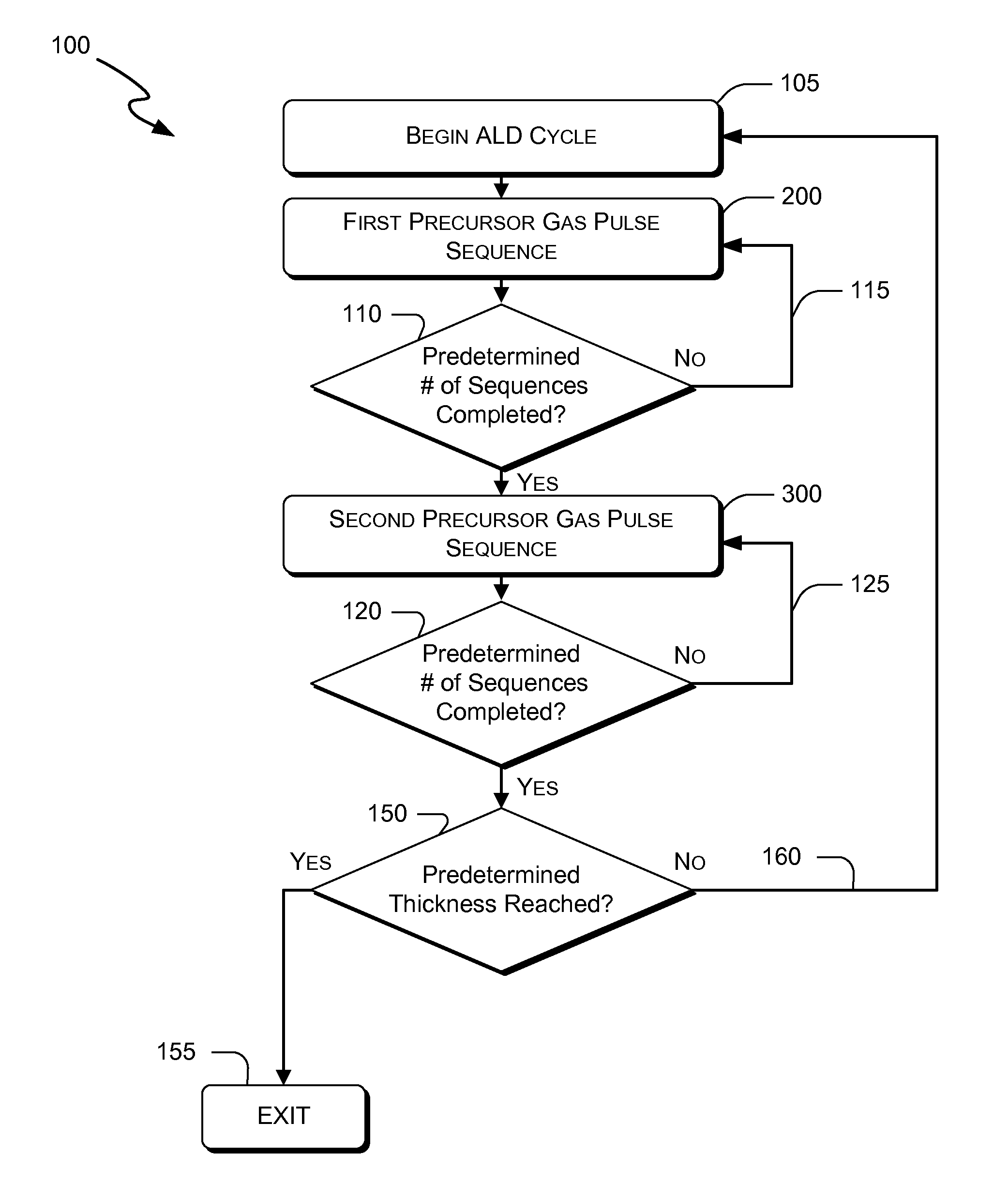
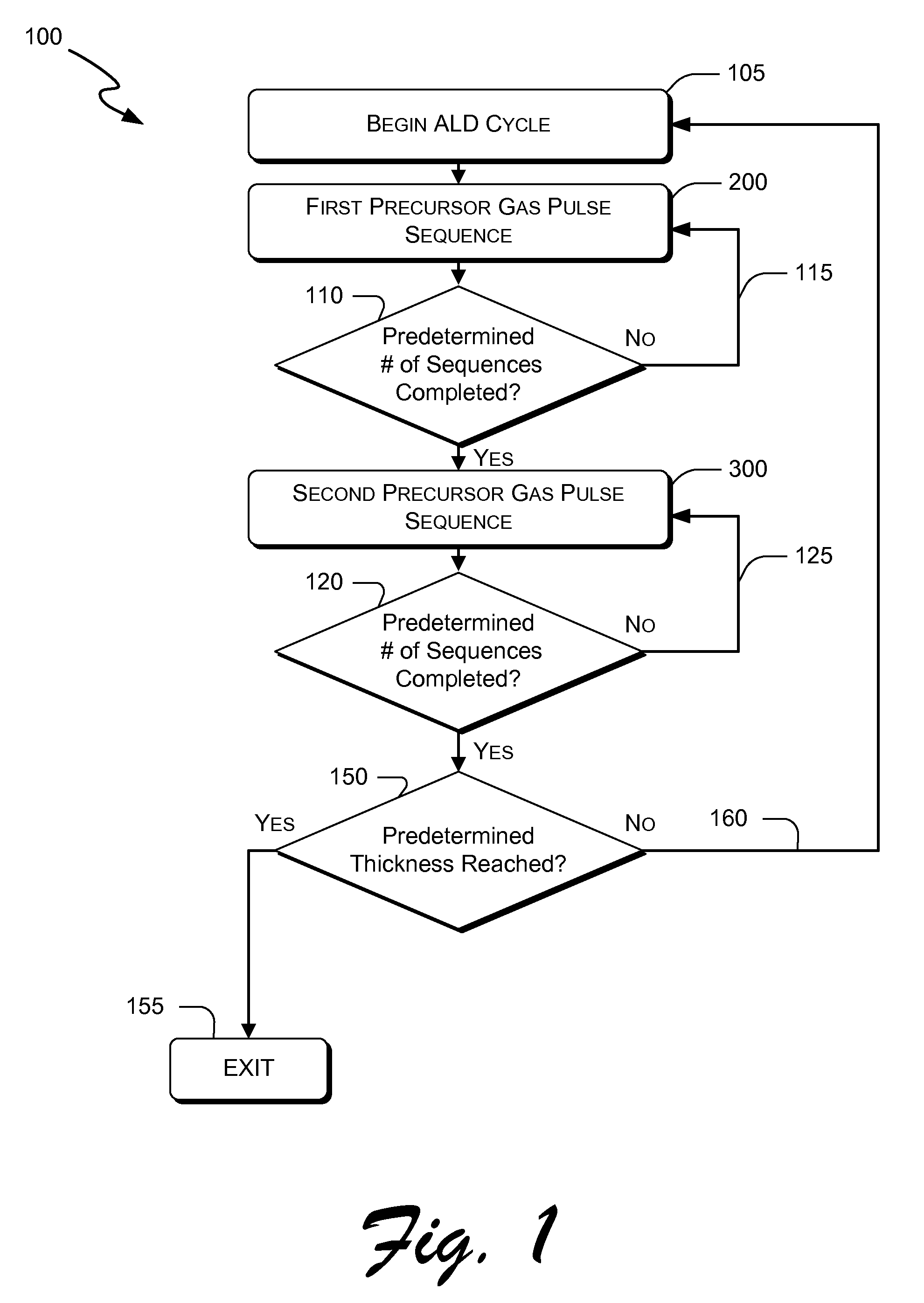
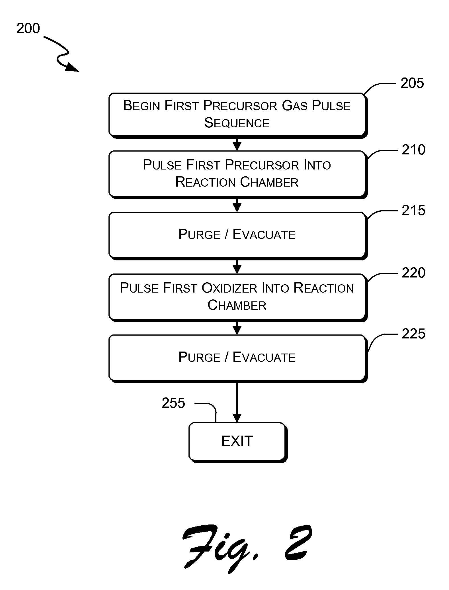
[0002]The present invention relates to thin film deposition, and more particularly methods using precursors to deposit hafnium lanthanum oxides by atomic layer deposition and components incorporating hafnium lanthanum oxide dielectric layers formed by methods consistent with the invention.

[0003]2. Background of the Invention

[0004]For many years, silicon dioxide (SiO2) has been used in semiconductor substrates for components such as transistor gate dielectrics and capacitor dielectrics. However, as circuit components have reduced in size, the electrical performance characteristics of SiO2 result in undesirable effects such as increased leakage current. Controlling leakage current to maintain high speed and low power performance presents a challenge when older-generation dielectrics such as SiO2 are used in the fabrication of newer integrated circuit geometries.

[0005]Newer processes, especially those that use fabrication geometries less than 65 nm have b...


PUM


Abstract

There is provided an improved method for depositing thin films using precursors to deposit binary oxides by atomic layer deposition (ALD) techniques. Also disclosed is an ALD method for depositing a high-k dielectric such as hafnium lanthanum oxide (HfLaO) on a substrate. Embodiments of the present invention utilize a combination of ALD precursor elements and cycles to deposit a film with desired physical and electrical characteristics. Electronic components and systems that integrate devices fabricated with methods consistent with the present invention are also disclosed.

Description

DESCRIPTION OF THE INVENTION[0001]1. Field of the Invention[0002]The present invention relates to thin film deposition, and more particularly methods using precursors to deposit hafnium lanthanum oxides by atomic layer deposition and components incorporating hafnium lanthanum oxide dielectric layers formed by methods consistent with the invention.[0003]2. Background of the Invention[0004]For many years, silicon dioxide (SiO2) has been used in semiconductor substrates for components such as transistor gate dielectrics and capacitor dielectrics. However, as circuit components have reduced in size, the electrical performance characteristics of SiO2 result in undesirable effects such as increased leakage current. Controlling leakage current to maintain high speed and low power performance presents a challenge when older-generation dielectrics such as SiO2 are used in the fabrication of newer integrated circuit geometries.[0005]Newer processes, especially those that use fabrication geome...

Claims


Application Information

Patent Timeline
Patent Type & Authority Patents(United States)
IPC IPC(8): H01L21/336
CPCH01L21/02181H01L21/02192H01L21/02194H01L21/0228H01L21/28194H01L21/28273H01L21/3141H01L21/31604H01L29/513H01L29/517H01L29/7881H01L29/40114H01L21/02189
Inventor RAISANEN, PETRI I.
Owner ASM IP HLDG BV
Learn More