Piezoelectric material and piezoelectric element

a piezoelectric element and piezoelectric material technology, applied in the field of piezoelectric materials, can solve problems such as temperature stability, safety of operators and the environment, and temperature stability problems, and achieve the effects of large piezoelectric constant, easy preparation, and lead-fr

Active Publication Date: 2012-01-24
SEIKO EPSON CORP
View PDF12 Cites 20 Cited by
  • Summary
  • Abstract
  • Description
  • Claims
  • Application Information

AI Technical Summary

Benefits of technology

[0014]In accordance with some aspects of the invention, it is possible to provide BiFeO3 and BaTiO3 based piezoelectric materials that are lead free and easy to prepare, yet still provide a large piezoelectric constant and a high Curie temperature.
[0016]According to the composition described above, the film performance can be improved by the spontaneous polarization of the material A, and a high Curie temperature can be maintained. Furthermore, the piezoelectric characteristics can be improved by the material B.
[0018]According to the composition described above, the piezoelectric characteristics can be improved by Ba(ZruTi1-u)O3 while maintaining the spontaneous polarization and high Curie temperature of Bi(Fe1-yMny)O3. In this manner, when the composition is within the range described above, the mixed materials preferentially exhibit their respective characteristics that are useful as a piezoelectric material, whereby the film characteristics can be improved.

Problems solved by technology

Unfortunately, PZT films contain lead (Pb), and therefore could pose problems for the safety of operators and the environment.
BaTiO3 has a large piezoelectric constant but has a low Curie temperature of about 120° C., and thus has a problem with temperature stability.
Many of the materials containing Bi have a high Curie temperature, but many of them have certain problems, such as a small dielectric constant and a small spontaneous polarization, as well as problems in temperature stability due to the phase transfer temperature being lower than the Curie temperature.
Other problems that may be encountered when using lead free piezoelectric materials for thin film piezoelectric elements include a compositional shift due to the fallout of alkali metal elements in materials containing such alkali metal elements, and diffusion into lower electrode layers due to the high temperature crystallization necessary for BaTiO3.
In either case, it is difficult to use these materials for thin film piezoelectric elements.
However, BiFeO3 has a small dielectric constant, and thus cannot be expected to achieve a high piezoelectric constant as a stand alone material.
However, when BaTiO3 is mixed too much, BaTiO3 becomes dominant and as a result the high Curie temperature and large spontaneous polarization of BiFeO3 cannot be best used.
Also, if piezoelectric elements are manufactured independently with either of the materials, BiFeO3 would likely result in a poor dielectric property, and BaTiO3 would deteriorate the piezoelectric characteristics since it is difficult to make its composition uniform, and thus would likely form layers with a lower dielectric constant.

Method used


Image

  • Piezoelectric material and piezoelectric element
  • Piezoelectric material and piezoelectric element
  • Piezoelectric material and piezoelectric element

Examples


embodiment 1

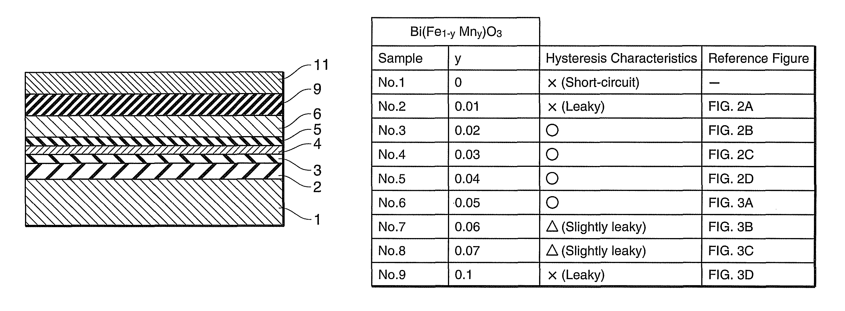
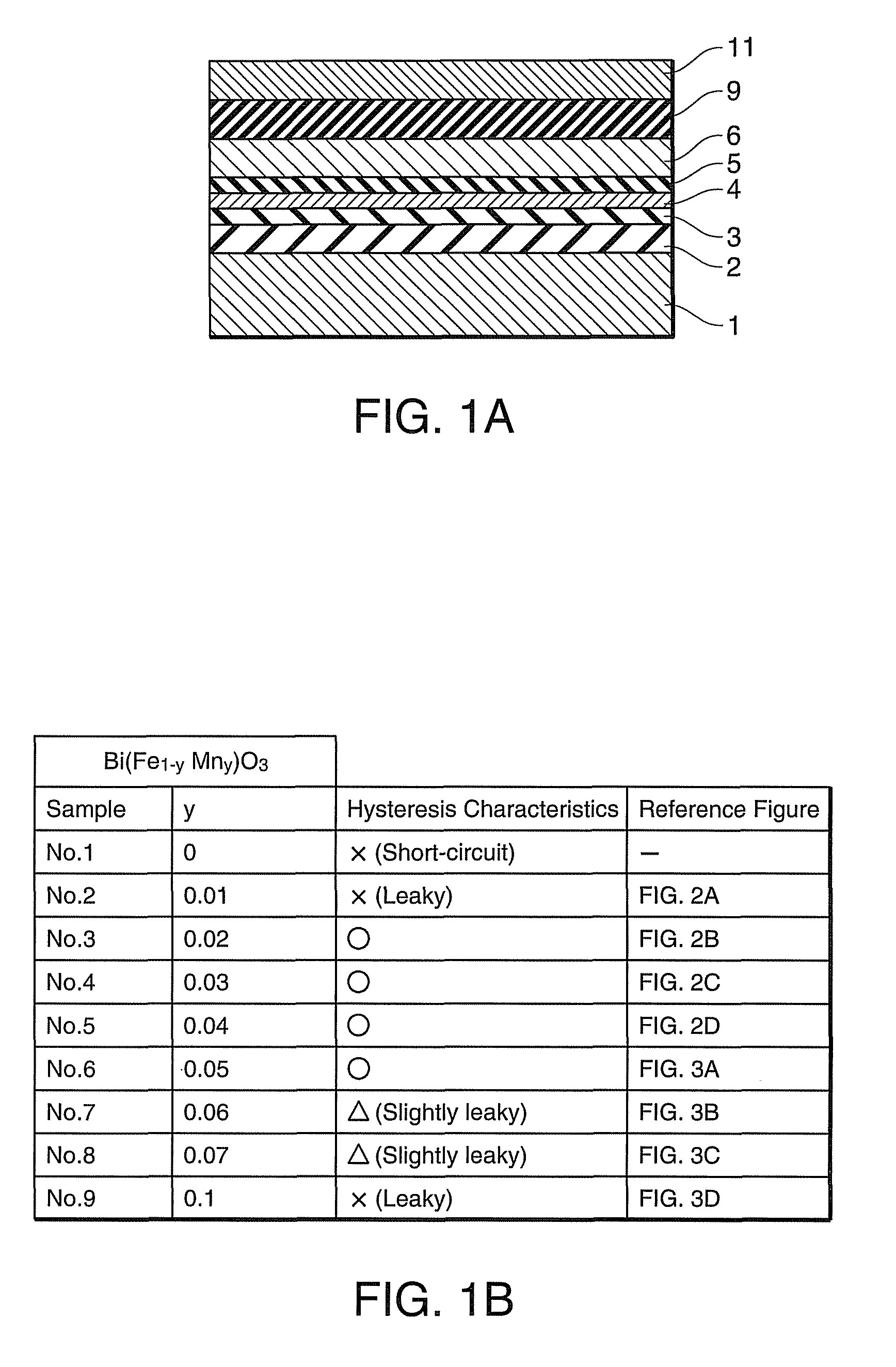
[0042]FIG. 1A is a cross-sectional view showing a step of a method for forming piezoelectric material in accordance with an embodiment of the invention. First, as shown in FIG. 1A, a substrate 1, such as, for example, a silicon (Si) substrate is prepared, and an elastic film (vibration plate) 2, such as, a silicon oxide film is formed on the surface of the substrate 1. The silicon oxide film may be formed by, for example, thermal oxidation to a film thickness of about 400 nm.

[0043]Then, on the elastic film 2, a TiAlN (titanium aluminum nitride) film 3 is formed by, for example, a RF sputter method to a film thickness of about 100 nm. Next, an Ir (iridium) film 4 is formed by a DC sputter method on the TiAlN film 3 to a film thickness of about 100 nm, and then an iridium oxide (IrO) film 5 is further formed thereon by a DC sputter method. The laminated films function as an adhesion layer between the silicon oxide film and the lower electrode, or function as a diffusion prevention lay...

embodiment example 1

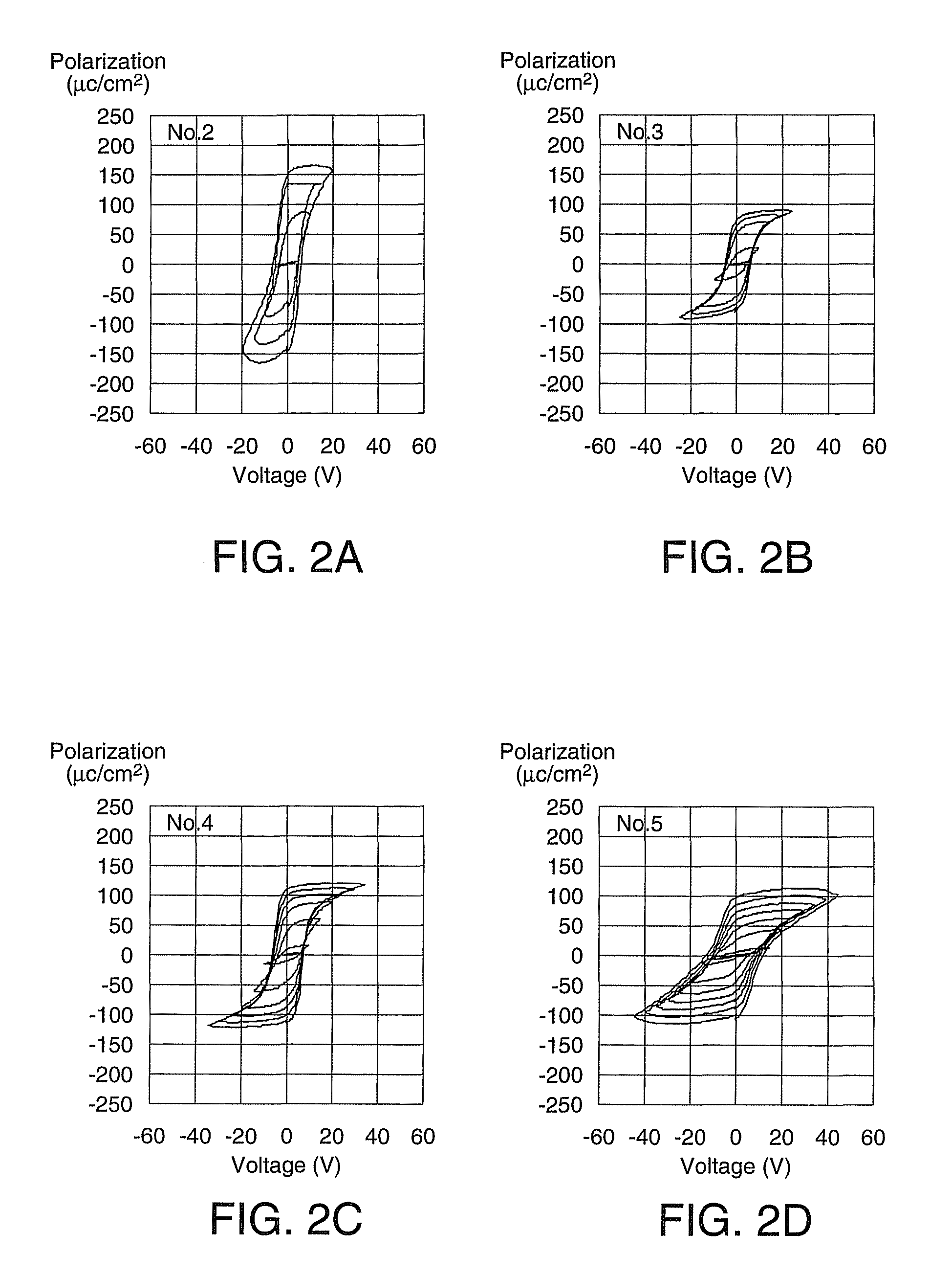
[0046]For example, a source material solution of Bi(Fe1-yMny)O3 adjusted to have an oxide concentration of 0.165 mol / kg is coated on a Pt film 6 by a spin coat method at 1500 rpm, thereby forming a precursor film. Then, the film is heat treated at 350° C. for three minutes, thereby drying and cleaning the film. The cleaning is conducted to thermally decompose organic compositions remaining in the precursor film into NO2, CO2, H2O and the like, and to remove them. The coating, drying and cleaning steps are repeated ten times, and then sintering (heat treatment) is conducted at 650° C. for ten minutes by using a lamp anneal furnace, thereby forming a Bi(Fe1-yMny)O3 film (the film 9) having a film thickness of about 400 nm. It is noted that the oxide concentration means a concentration of Bi(Fe1-yMny)O3 that is an oxide in this case.

[0047]Then, on the Bi(Fe1-yMny)O3 film (9), a conductive film, such as, for example, a Pt film is deposited by a DC sputter method to a thickness of about ...

embodiment example 2

[0052]In this embodiment example, structures (see FIG. 1A) described above were formed by a process similar to that of Embodiment Example 1, using a source material solution in which the value x in films of (1−x)Bi(Fe1-yMny)O3-xBa(ZruTi1-u)O3 was adjusted in the range between 0 and 0.5, and the dielectric characteristics of the structures were examined. It is noted that the value y and the value u were fixed at y=0.05 and u=0. In other words, mixed crystals of Bi(Fe, Mn)O3 and Ba(Ti)O3 were formed using a source material solution of (1−x)Bi(Fe0.95Mn0.05)O3-xBaTiO3.

[0053]FIG. 4 is a table showing the pass and fail results of the hysteresis characteristics of samples No. 10-No. 15 whose composition ratios x were adjusted, respectively. FIGS. 6A-5D and FIGS. 6A-6B are graphs showing the hysteresis characteristics of the samples, respectively. It is noted that sample No. 10 is the same as sample No. 6.

[0054]As shown in FIG. 4 through FIG. 6B, it is clear that samples No. 14 and No. 15 w...


PUM

PropertyMeasurementUnit
Curie temperatureaaaaaaaaaa
Tcaaaaaaaaaa

Abstract

A piezoelectric element includes a first electrode, a piezoelectric film disposed on the first electrode, and a second electrode disposed on the piezoelectric film. The piezoelectric film is composed of piezoelectric material that is lead free and formed by mixing 100(1−x)% of material A having a spontaneous polarization of 0.5 C / m2 or greater at 25° C. and 100 x % of material B having piezoelectric characteristics and a dielectric constant of 1000 or greater at 25° C., wherein (1−x)Tc(A)+xTc(B)≧300° C., where Tc(A) is the Curie temperature of the material A and Tc(B) is the Curie temperature of the material B.

Description

BACKGROUND[0001]1. Technical Field[0002]The present invention relates to piezoelectric materials that are used for piezoelectric elements.[0003]2. Related Art[0004]Piezoelectric elements possess a characteristic in which crystals are charged when they are deformed, or they are deformed when they are placed in an electric filed. As such, they are commonly used for liquid jet apparatuses such as ink jet printers.[0005]Piezoelectric thin films such as PZT (lead titanate zirconate: Pb(ZrxTi1-x)O3) films have been widely used for such piezoelectric elements.[0006]Unfortunately, PZT films contain lead (Pb), and therefore could pose problems for the safety of operators and the environment. Accordingly, research and development regarding lead free piezoelectric materials are being extensively conducted. For example, Japanese Laid-open Patent Applications JP-A-2004-6722, JP-A-2007-266346 and JP-A-2007-287745 describe lead free piezoelectric materials.[0007]Among the aforementioned piezoelect...

Claims


Application Information

Patent Timeline
Patent Type & Authority Patents(United States)
IPC IPC(8): H01L41/09H01L41/18H01L41/22H01L41/257H01L41/39
CPCB41J2/14233B41J2/161B41J2/1645B41J2/045H01L41/18H01L41/0815H01L41/1878H01L41/318H10N30/10516H10N30/8561H10N30/078H10N30/85
Inventor HAMADA, YASUAKIKIJIMA, TAKESHI
Owner SEIKO EPSON CORP
Why Eureka
Try Eureka