Feedforward/feedback litho process control of stress and overlay

a lithographic process and stress technology, applied in the field of substrate processing, can solve the problems of poor sensitivity and signal-to-noise ratio, poor method convenience in production environment, complex apparatus for raman spectroscopy, etc., and achieve the effects of reducing patterning errors, high precision, and improving yield

Active Publication Date: 2012-02-07
KLA CORP
View PDF21 Cites 20 Cited by
  • Summary
  • Abstract
  • Description
  • Claims
  • Application Information

AI Technical Summary

Benefits of technology

[0025]Embodiments of the present invention utilize various methods of stress, topography (shape) and overlay metrology in both feed-forward and feedback control loops with patterning, deposition and thermal processing tools in order to enhance die yield in semiconductor device manufacture. By automatically adjusting the patterning step to compensate for variations in prior processing steps, the maximum yield may be obtained from each wafer even when the stress from a given process changes over time or is non-uniform across the wafer. Unlike the prior art, embodiments of the present invention utilize direct feedback or feed forward of high order wafer and field level stress or topography metrology data as a means of controlling patterning, deposition and thermal processing tools. The prior art, by contrast, relied on keeping a global (or wafer average) stress introduced at each process step below some (process-specific) predetermined control limit in order to maintain the overall stress level. Just measuring a global or average stress value cannot reliably catch all local deviations in stress since a large stress in a small area may have only a small effect on the global stress, or large positive and negative local stresses in different areas may partially cancel each other out leading to low average stress. Furthermore since the distortions at any location on the wafer are the result of the net effect of all the prior processing steps, tight control limits may need to be imposed on each individual step to avoid cumulative effects at some wafer location causing unacceptable distortions. Imposing a low global stress control limit on a process step in order to avoid stress accumulating over multiple steps as well as to ensure a reduced probability of local stress exceeding some threshold may result in a more expensive and less efficient manufacturing process. Low control limits may require frequent adjustments to the process tools in order to keep them within that limit resulting in a less time available on the process tool for processing wafers and hence low productivity or the a need to purchase more processes tools than otherwise necessary to compensate for the reduced productivity.
[0041]In embodiments of the present invention, the metrology tool 110 may measure wafer stress and / or topography at critical process steps with more detail (spatial resolution) than is current practice. As discussed above, the typical prior art practice is only to monitor a wafer average stress. In embodiments of the present invention, by contrast, wafer stress may be monitored at a resolution of one, or a few, mm (e.g., about one millimeter to about five millimeters) as required to make an accurate prediction of the interaction with the chuck. These more detailed measurements are combined with models of how these stresses or shape changes interact with the patterning tool wafer chuck in order to feed high-order correctables 207 to the patterning tool 120. As a result, the patterning tool can make real-time adjustments during scanning in order to produce better registration between the printed pattern and prior patterns on the substrate 101. No such modeling or feed-forward scheme is used in prior art wafer processing systems.
[0048]Embodiments of the present invention can reduce patterning errors and improve yield for processes that require high precision and small design rules.

Problems solved by technology

These other methods are generally less convenient for use in a production environment than the change in wafer shape metrology just described because these other techniques are generally slower or require more expensive hardware.
But the slowness of the measurement and the complexity of the apparatus make this more suitable for use as a reference technique than as a routine production metrology technique that needs to measure tens or hundreds of wafers per day.
The apparatus for Raman spectroscopy is complex compared with that for shape measurement, and the sensitivity and signal-to-noise ratio are poor because the Raman lines in semiconductors are so weak relative to the incident laser line.
For all of these reasons Raman is not suitable for routine production measurements.
As the depth of focus and overlay control required for the smallest dimensions printed on the wafer shrink, simply controlling global wafer stress below some threshold is no longer sufficient.
However, the laser is typically not powerful enough to heat the whole surface simultaneously.
Non-uniform stresses in a wafer can distort the local shape of the wafer in complex ways.
For example, the wafer may bend both in-plane and out of plane as a result of non-uniform stresses.
The time available to make these measurements is limited because these measurements have to be done while the previous wafer is being exposed (or otherwise processed).
Consequently, the number of measurements that can be made during such time is limited.
However, if the changes in stress are non-uniform then the shape changes are complex and linear models may not be accurate enough.
Scanners do adjust the leveling of each individual die before printing, but the leveling only corrects for average slopes in the X and Y directions (e.g., a tilted wafer plane) and not for vertical distortions on scale lengths shorter than a die.
The complex distortions of the shape of the wafer in X, Y and possibly Z on the chuck due to the non-uniform changes in stress are not adequately accounted for by the patterning tool leading to regions of the wafer where yield is low due to poor alignment of one pattern with earlier patterns on chips in that area of the wafer.

Method used


Image

  • Feedforward/feedback litho process control of stress and overlay
  • Feedforward/feedback litho process control of stress and overlay
  • Feedforward/feedback litho process control of stress and overlay

Examples


Embodiment Construction

[0023]Although the following detailed description contains many specific details for the purposes of illustration, anyone of ordinary skill in the art will appreciate that many variations and alterations to the following details are within the scope of the invention. Accordingly, the exemplary embodiments of the invention described below are set forth without any loss of generality to, and without imposing limitations upon, the claimed invention.

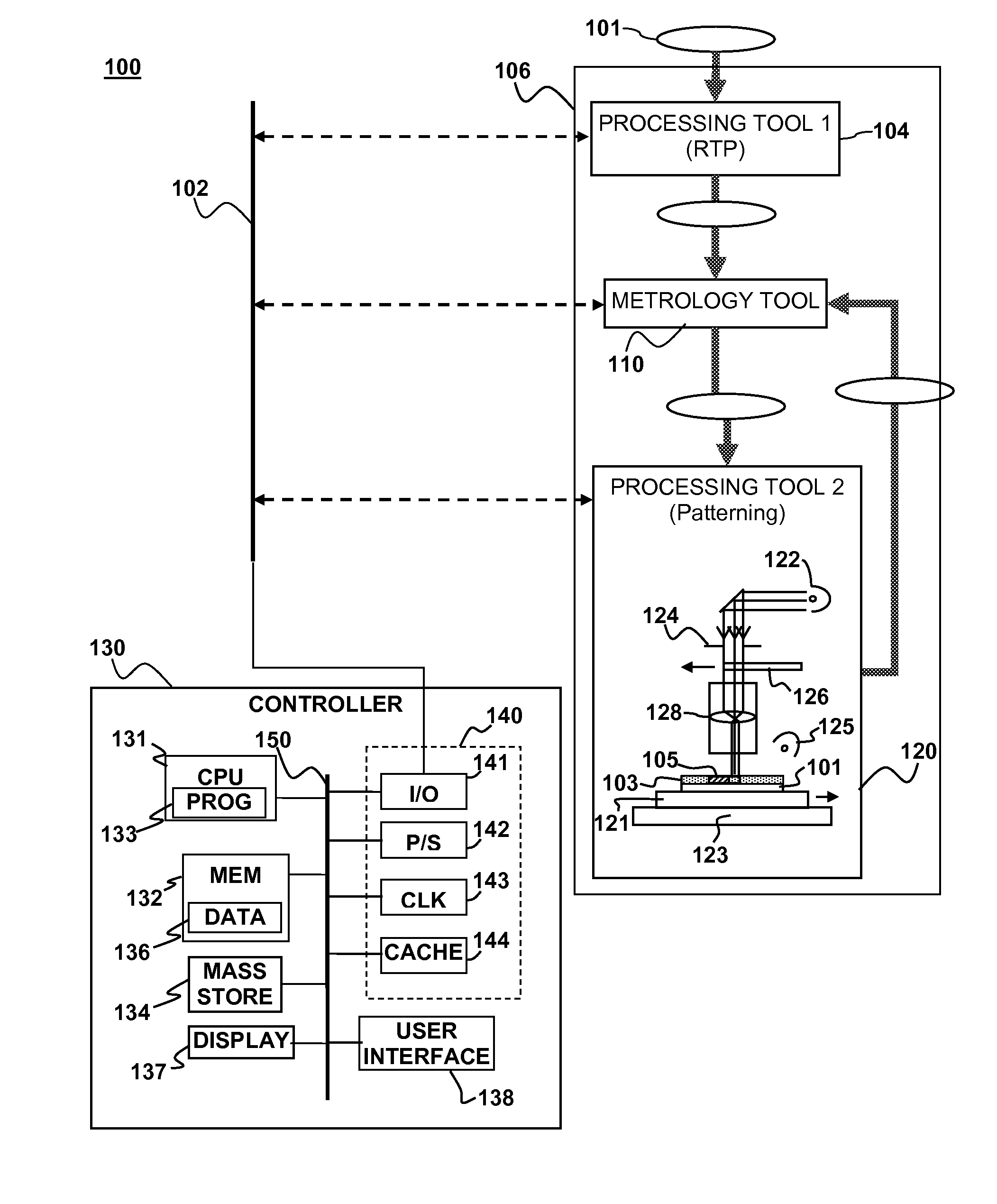
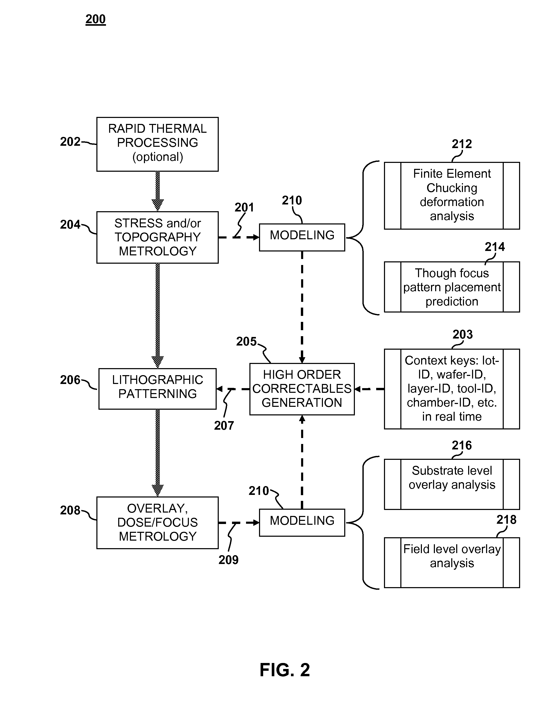
[0024]Embodiments of the present invention include a method and apparatus for process control in a lithographic process are described. Metrology may be performed on a substrate either before or after performing a lithographic patterning process on the substrate. One or more correctables to the lithographic patterning process may be generated based on the metrology. The lithographic patterning process performed on the substrate (or a subsequent substrate) may be adjusted with the correctables.

[0025]Embodiments of the present invention utilize...


PUM


Abstract

A method and apparatus for process control in a lithographic process are described. Metrology may be performed on a substrate either before or after performing a lithographic patterning process on the substrate. One or more correctables to the lithographic patterning process may be generated based on the metrology. The lithographic patterning process performed on the substrate (or a subsequent substrate) may be adjusted with the correctables.

Description

CLAIM OF PRIORITY[0001]This application claims the benefit of priority of commonly-assigned co-pending U.S. Provisional Patent Application No. 60 / 940,953, filed May 30, 2007, the entire contents of which are incorporated herein by reference.FIELD OF THE INVENTION[0002]This invention generally relates to substrate processing and more particularly to process control in a lithographic process.BACKGROUND OF THE INVENTION[0003]Various methods of measuring the stress in films deposited on semiconductor wafers are known in the art. Most commonly, the measurement is performed by measuring the shape of the wafer before a process step and then repeating the shape measurement after the process step. The stress of a film deposited (or removed) during the process step is calculated from the change in shape of the wafer and the known elastic modulus of the semiconductor material comprising the bulk of the wafer. The thickness of the wafer and / or film may be known prior to the shape measurement, o...

Claims


Application Information

Patent Timeline
Patent Type & Authority Patents(United States)
IPC IPC(8): G03B27/42
CPCG03F7/70258G03F7/705G03F7/70783G03F7/70616G03F7/70525G03F7/70608
Inventor ADEL, MICHAELFIELDEN, JOHNWIDMANN, AMIRROBINSON, JOHNCHOI, DONGSUB
Owner KLA CORP
Why Eureka
Try Eureka