High-density, trench-based non-volatile random access SONOS memory SOC applications

a sonos memory and trench technology, applied in semiconductor devices, electrical equipment, instruments, etc., can solve the problems of difficult to provide the high voltage level necessary for floating gate operation, severely limit the battery life, and difficult to integrate floating gate memories with complementary metal oxide semiconductors (cmos), so as to reduce the minimum feature size, prevent short-channel behavior of select gate, and scale easily

Active Publication Date: 2012-02-21
GLOBALFOUNDRIES US INC
View PDF20 Cites 27 Cited by
  • Summary
  • Abstract
  • Description
  • Claims
  • Application Information

AI Technical Summary

Benefits of technology

[0009]Specifically, the present invention provides two-transistor (2-Tr) SONOS memory cells with randomly accessible storage locations. In one embodiment, the memory transistor is a planar device located on a surface of a semiconductor substrate, while the select transistor is located within a trench structure that is present in the semiconductor substrate. In this embodiment of the present invention, a “shallow” trench structure (on the order of from about 1 to about 2 μm in depth) is used to serve as the select gate—or in other words—the cell's access field effect transistor (FET) lies along the vertical sidewall of a trench structure. Short-channel behavior of the select gate can be prevented as the trench depth, which determines the channel length of the cell, can be made larger without affecting the areal density of the cell. Because the select MOSFET is formed along the sidewall of a trench, its channel length is not constrained to scale with decreasing minimum feature size of successive technology nodes; however, the trench cross-section dimensions can easily scale with the minimum feature size of the technology node, thus avoiding area penalty. It has been estimated that a 2-Tr SONOS cell designed in a 65 nm logic library could be on the order of 0.15 μm2—this would be approximately 5× smaller than any 2-Tr memory cell that is currently in the marketplace.
[0010]Additional benefits that are provided in the first embodiment of the present invention include: (1) the operation of the memory cell uses voltages that are half that of presentday flash memories, which should provide higher margin for oxide reliability of memory cells, (2) inherently superior read, e.g., disturb characteristics, compared to 1-Tr NORs—as the memory FET is not biased during a read operation. Moreover, the number of additional masks needed to integrate the SONOS trench cells into CMOS is estimated to be a maximum of 4.
[0011]The trench structure is the key enabler in providing these much-reduced 2-Tr SONOS cell sizes. However, unlike the trench structures in embedded dynamic random access memory (eDRAM) technology, the depth for the trench structure of the present invention is much shallower. The depth of the trench structure would only need to accommodate a channel length that would minimize detrimental short-channel effects; it is estimated that trench depths of about 0.5 μm to about 1.0 μm would be sufficient for this purpose.
[0023]In a second embodiment of the present invention, the memory transistor and the select gate transistor are both located within a trench structure that is formed into a semiconductor substrate. In this embodiment, a SONOS memory trench memory cell is provided that can be scaled to approximately ½ the current SONOS cell sizes in the 65 nm logic generation and only a single mask process above the CMOS process is used. Essentially, the SONOS trench memory cell described in the second embodiment decouples the standard CMOS process from the processing of the non-volatile random access memory storage and access elements. The key enabler in this embodiment is that the select gate and the memory gate are integrated with a trench structure. The trench structure typically has a depth, as measured from the top surface of the semiconductor substrate to the bottom trench wall, from about 1 to about 2 μm. The relatively shallow trench depth (as compared to 8 μm depths of DRAM storage capacitors) easily accommodates both the select and memory transistors which are relatively immune from short channel effects that challenge the CMOS logic devices. Here, the select gate is grown in a bottom portion of the trench structure and the memory transistor comprising an ONO film is formed in the upper portion of the trench structure. By allowing for the select and memory gates to be combined within a trench structure, one can shrink the cell to cell sizes of approximately 0.07-0.09 μm2 in the 65 nm logic technology. In addition, both the trench SONOS select gate and the memory gate formation can be fully decoupled from normal CMOS processing—no special block masks are needed to create different gate dielectrics and one could fully optimize memory cell functionality without compromising logic performance. The implementation of a trench SONOS cell into a CMOS logic technology would only add one mask to the base logic process.

Problems solved by technology

Because of the necessity of providing high voltage levels for floating gate memory operation, integration of floating gate memories with complementary metal oxide semiconductor (CMOS) is problematic.
At these low supply voltages, it is difficult to provide high voltage levels necessary for floating gate operation—even with the use of charge-pumping circuits.
For mobile applications, the high supply voltages necessary for conventional floating gate memories severely limit the battery life.
Moreover, there is a severe cost penalty of integrating floating gate memories with CMOS—it is estimated that as many as nine (9) additional lithography steps may be necessary.
However, SONOS cells are not immune to scaling concerns.
The moderate voltages needed for programming put limits on the transistor design one can employ.
Short-channel effects, including punch-through, can easily occur even at these voltages, if the device channel lengths are too short.
Increasing channel doping concentrations to deter punch-through can lead to lower junction breakdown and destruction of any memory capability.
The scaling of SONOS memory cells has been limited to planar devices.
Although smaller in size, the planar cell has its limits as the channel length may be more difficult to scale in the forthcoming generations.
Due to the necessity of separating the SONOS memory gate to CMOS processing, integration with high-performance CMOS can become costly.

Method used


Image

  • High-density, trench-based non-volatile random access SONOS memory SOC applications
  • High-density, trench-based non-volatile random access SONOS memory SOC applications
  • High-density, trench-based non-volatile random access SONOS memory SOC applications

Examples


first embodiment

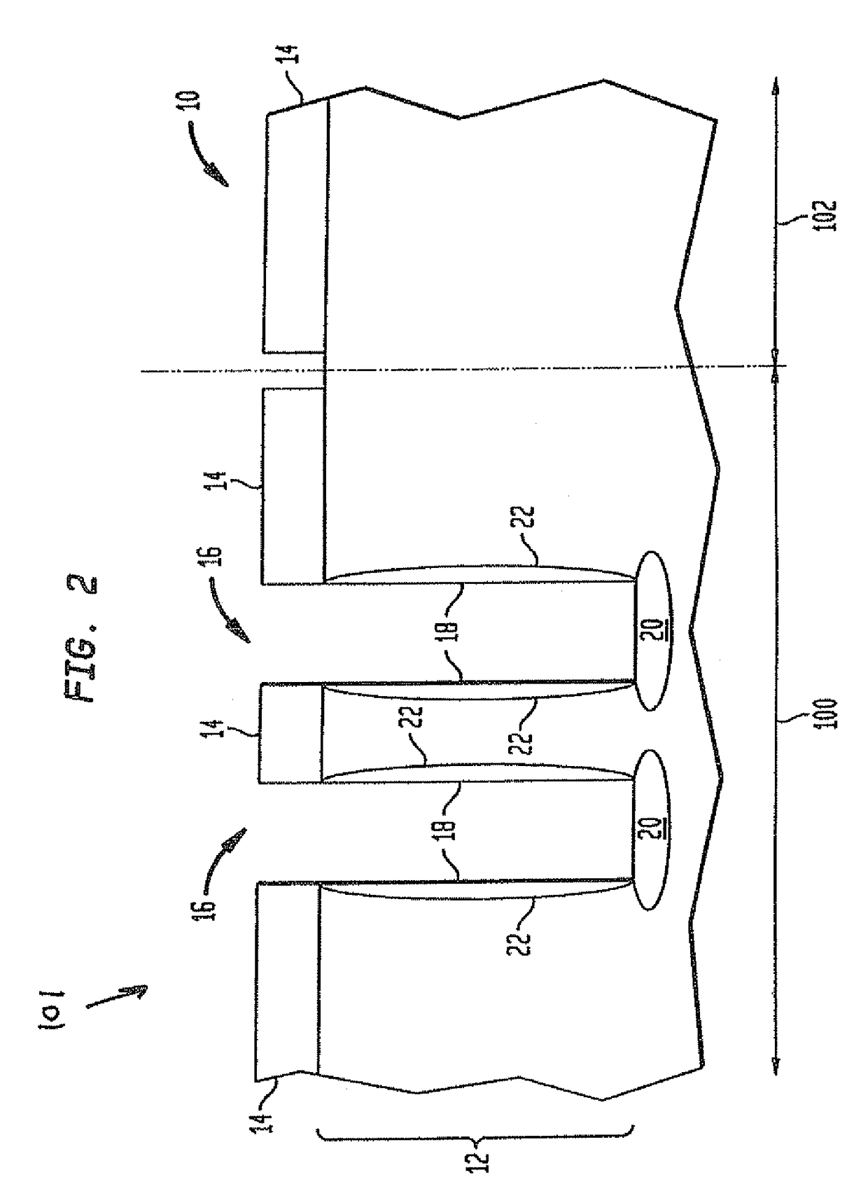
[0051] 2-TR SONOS memory cell wherein the select gate is located within a trench structure and the memory gate is located on a surface of a semiconductor substrate including the trench structure.

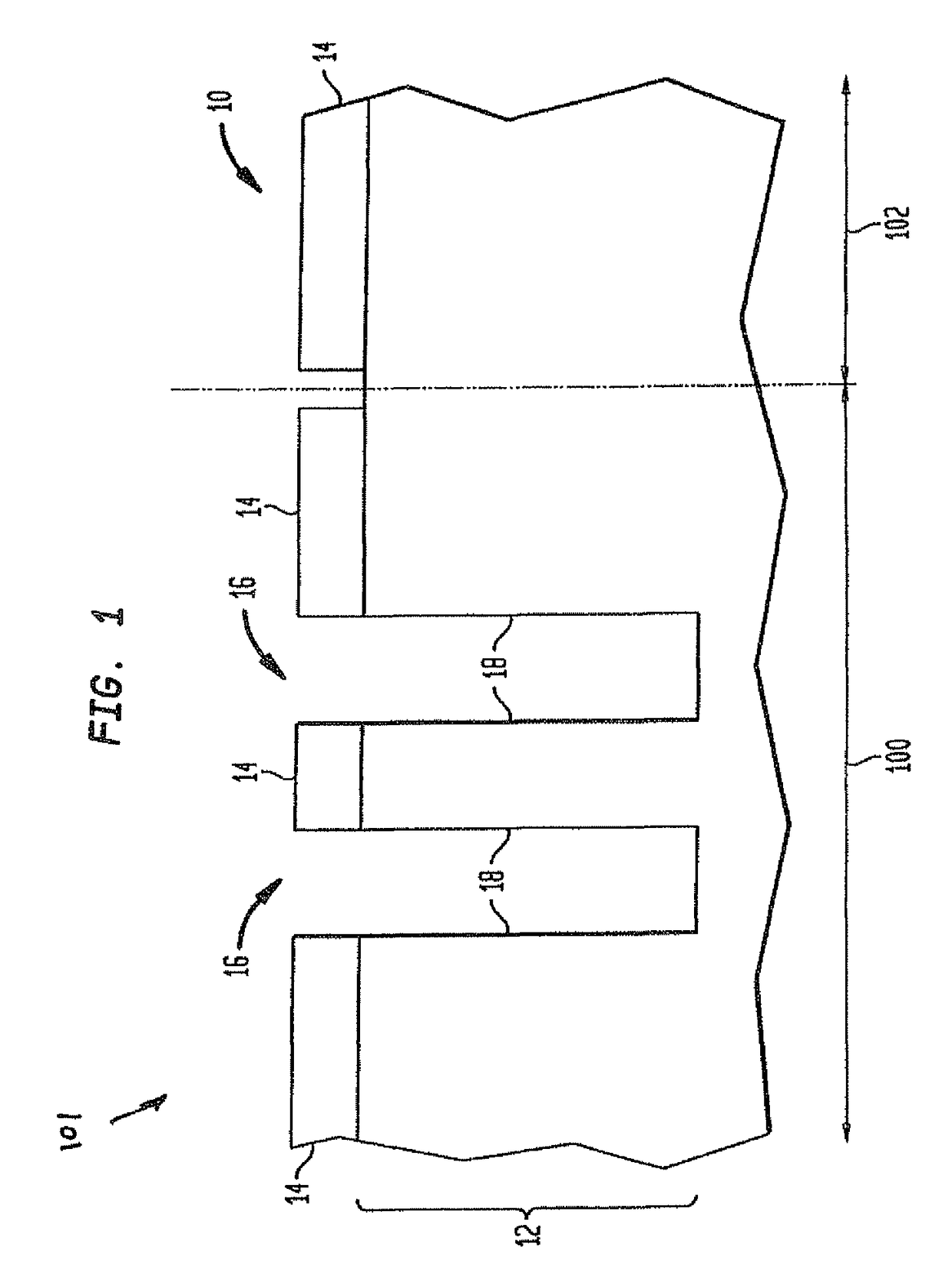
[0052]The first embodiment of fabricating the inventive 2-Tr SONOS memory cell begins with providing a structure 10 such as shown in FIG. 1 which includes at least one array region 100 and at least one region 102 that lies to the periphery of the at least one array region 100. Region 102 is referred to herein as an array periphery. The structure 10 shown in FIG. 1 comprises a semiconductor substrate 12 including a pad stack 14 having a plurality of openings 16 on top of the substrate 12 in the array region 100. In the array region 100, the structure 10 also includes trench structures 18 that are located in the semiconductor substrate 12. It is noted that the semiconductor substrate 12 in the periphery array region 102 is protected with a blanket layer of the pad stack 14.

[0053]The semiconduc...

second embodiment

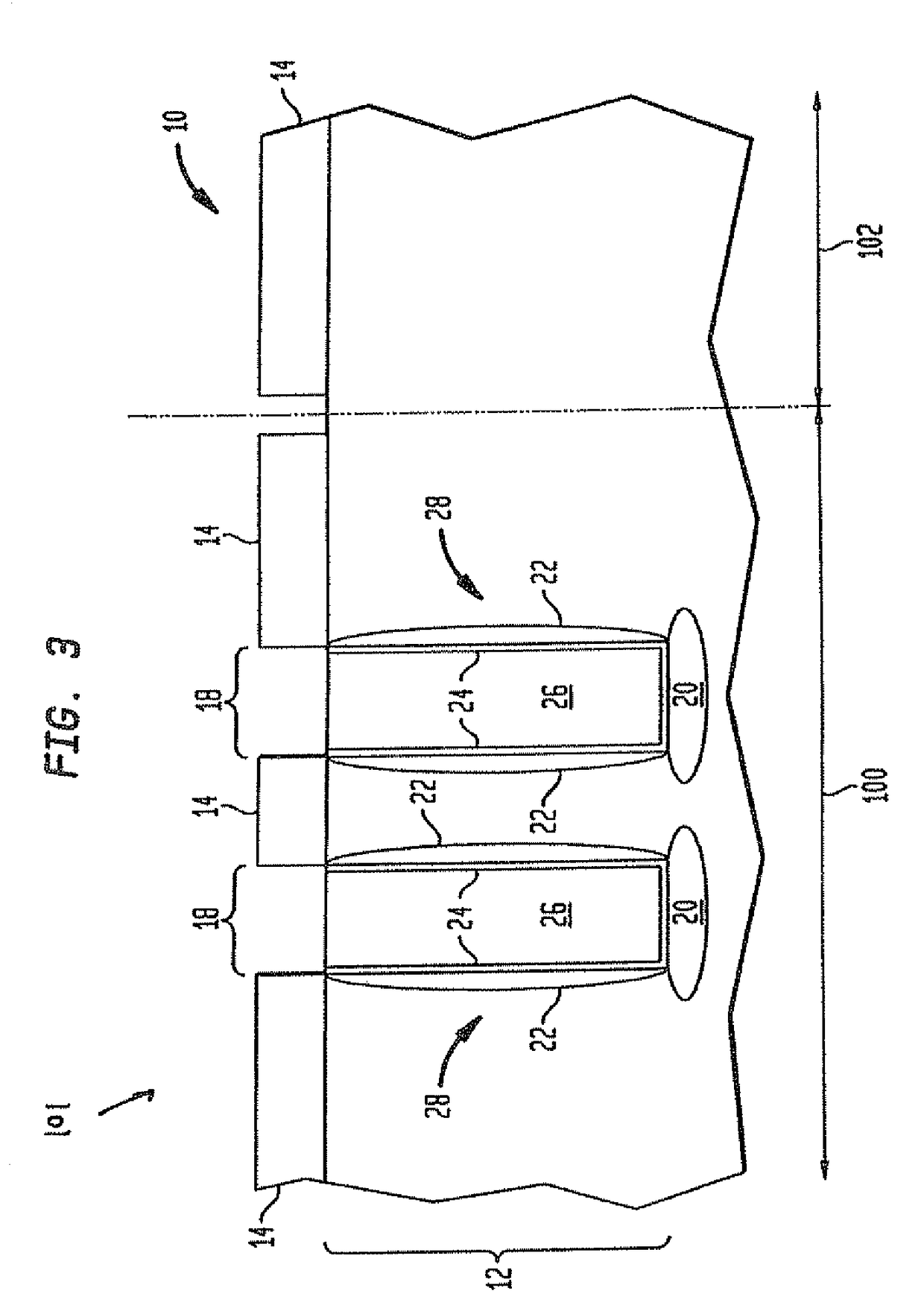
[0080] 2-Tr SONOS wherein the select gate and the memory gate are both located within a trench structure that is formed into a semiconductor substrate.

[0081]This second embodiment of the present invention offers the following advantages: (1) The trench structure memory gate can be created prior to CMOS processing and can be truly integrated into CMOS processing. The ONO dielectric comes before the CMOS process and can be optimized without degrading the CMOS device. (2) The trench structure memory select gate is structurally shallower than prior art eDRAM trenches (1-2 μm tops) and it can be formed using simplified processing, e.g., oxidation for the select gate, resist recess process, ONO formation and a one trench process (fill, planarization and recessing). (3) Extremely small cell sizes can be achieved (on the order of about 0.07 to 0.09 μm2.

[0082]The second embodiment of the present invention begins by utilizing the processing steps described above in forming the structure shown...


PUM


Abstract

The present invention provides two-transistor silicon-oxide-nitride-oxide-semiconductor (2-Tr SONOS) non-volatile memory cells with randomly accessible storage locations as well as a design structure including the semiconductor memory devices embodied in a machine readable medium. In one embodiment, a 2-Tr SONOS cell is provided in which the select transistor is located with a trench structure having trench depth from 1 to 2 μm and the memory transistor is located on a surface of a semiconductor substrate adjoining the trench structure. In another embodiment, a 2-Tr SONOS memory cell is provided in which both the select transistor and the memory transistor are located within a trench structure having the depth mentioned above.

Description

[0001]This application is related to co-pending and co-assigned U.S. patent application Ser. No. 10 / 907,686, filed Apr. 12, 2005, currently pending.FIELD OF THE INVENTION[0002]The present invention relates to semiconductor memory devices. More particularly, the present invention relates to two-transistor (2-Tr) semiconductor-oxide-nitride-oxide-semiconductor (SONOS) trench memory cells with randomly accessible storage locations and a design structure including the semiconductor memory devices embodied in a machine readable medium. The present invention provides 2-Tr SONOS trench memory cells wherein the select gate is located in a trench structure and the memory gate is located on a surface of a semiconductor substrate or wherein both the select gate and the memory gate are located in a trench structure.BACKGROUND OF THE INVENTION[0003]Conventional flash memory products employing floating gate technologies, where the memory state is represented by the charge stored in an insulated, ...

Claims


Application Information

Patent Timeline
Patent Type & Authority Patents(United States)
IPC IPC(8): H01L29/76
CPCH01L27/11565H01L27/11568H01L27/1157G11C16/0433H10B43/10H10B43/30H10B43/35
Inventor HO, HERBERT L.MANDELMAN, JACK A.NING, TAK H.OTANI, YOICHI
Owner GLOBALFOUNDRIES US INC
Why Eureka
Try Eureka