Amplification type solid-state imaging device

a solid-state imaging and amplifier technology, applied in the direction of radio frequency controlled devices, instruments, television systems, etc., can solve the problems of exceeding the power voltage vd, difficult to achieve the voltage vfd of the signal charge accumulating portion b>203, etc., to facilitate the completion of the transfer and achieve high-quality images.

Active Publication Date: 2012-03-27
SHARP KK
View PDF15 Cites 2 Cited by
  • Summary
  • Abstract
  • Description
  • Claims
  • Application Information

AI Technical Summary

Benefits of technology

[0017]According to the above construction, by lowering the drain side voltage of the amplifying transistor by the control section before resetting, the source side of the amplifying transistor connected directly to the read signal line can be made to have a first voltage in a low state. Subsequently, by turning on the reset transistor for a prescribed period to reset the voltage of the signal charge accumulating portion and thereafter raising the drain side voltage of the amplifying transistor to make the drain side of the amplifying transistor have a high voltage, the read signal line can be made to have a second voltage higher than the first voltage. By so doing, the voltage of the signal charge accumulating portion is made higher than the voltage immediately after the resetting via the capacitance between the input side and the output side (read signal line side) of the amplifying transistor. If the transfer transistor is turned on in this state, it becomes possible to sufficiently secure a voltage difference between the photoelectric transducer and the signal charge accumulating portion (FD) and to easily achieve complete transfer, and this enables the achievement of no residual image. Moreover, by expanding the voltage margins of the photoelectric transducer and the signal charge accumulating portion, the pixel performance can be improved with an increase in the maximum amount of signals to be handled.
[0026]According to the above embodiment, by raising the drain side voltage of the amplifying transistor by the control section to make the read signal line have the second voltage and thereafter turning on the transfer transistor to transfer the signal charge from the photoelectric transducer to the signal charge accumulating portion, the charge transfer from the photoelectric transducer to the signal charge accumulating portion can be made complete.
[0035]According to the above embodiment, the capacitance between the input side and the output side (on the read signal line side) of the amplifying transistor increases because of the capacitance due to the capacitance element added to the capacitance between the gate and the source of the amplifying transistor. The effect of raising the voltage of the signal charge accumulating portion from the voltage at the time of resetting is increased when the voltage of the read signal line rises. This therefore further facilitates the completing (=no residual image) of the charge transfer from the photoelectric transducer to the signal charge accumulating portion.
[0037]According to the above embodiment, by employing the depletion type MOS type transistor for the reset transistor, the voltage of the signal charge accumulating portion can be raised up to the power voltage when the signal charge accumulating portion is reset by the low first voltage of the read signal line. Therefore, when the read signal line is subsequently made to have the second voltage higher than the first voltage, the voltage of the signal charge accumulating portion can be raised up to a value higher than the power voltage. This therefore becomes more advantageous for the completing (=no residual image) of the charge transfer from the photoelectric transducer to the signal charge accumulating portion.
[0044]According to the above embodiment, the embedded type photodiode is completely depleted during the charge transfer from the photoelectric transducer to the signal charge accumulating portion, and this facilitates the completing of the transfer and allows a high-quality image to be obtained.
[0045]As is apparent from the above, the amplification type solid-state imaging device of the invention can make the voltage of the signal charge accumulating portion higher than the power voltage in the reset operation and easily achieve complete transfer (=no residual image) of the signal charge from the photoelectric transducer to the signal charge accumulating portion by sufficiently securing the voltage difference between the embedded photodiode and the signal charge accumulating portion (FD) when the transfer transistor is turned on.

Problems solved by technology

However, the method of Document 1 has the following problem.
Therefore, it is difficult for the value of the voltage VFD of the signal charge accumulating portion 203 to exceed the power voltage Vd.

Method used


Image

  • Amplification type solid-state imaging device
  • Amplification type solid-state imaging device
  • Amplification type solid-state imaging device

Examples


first embodiment

[0056](First Embodiment)

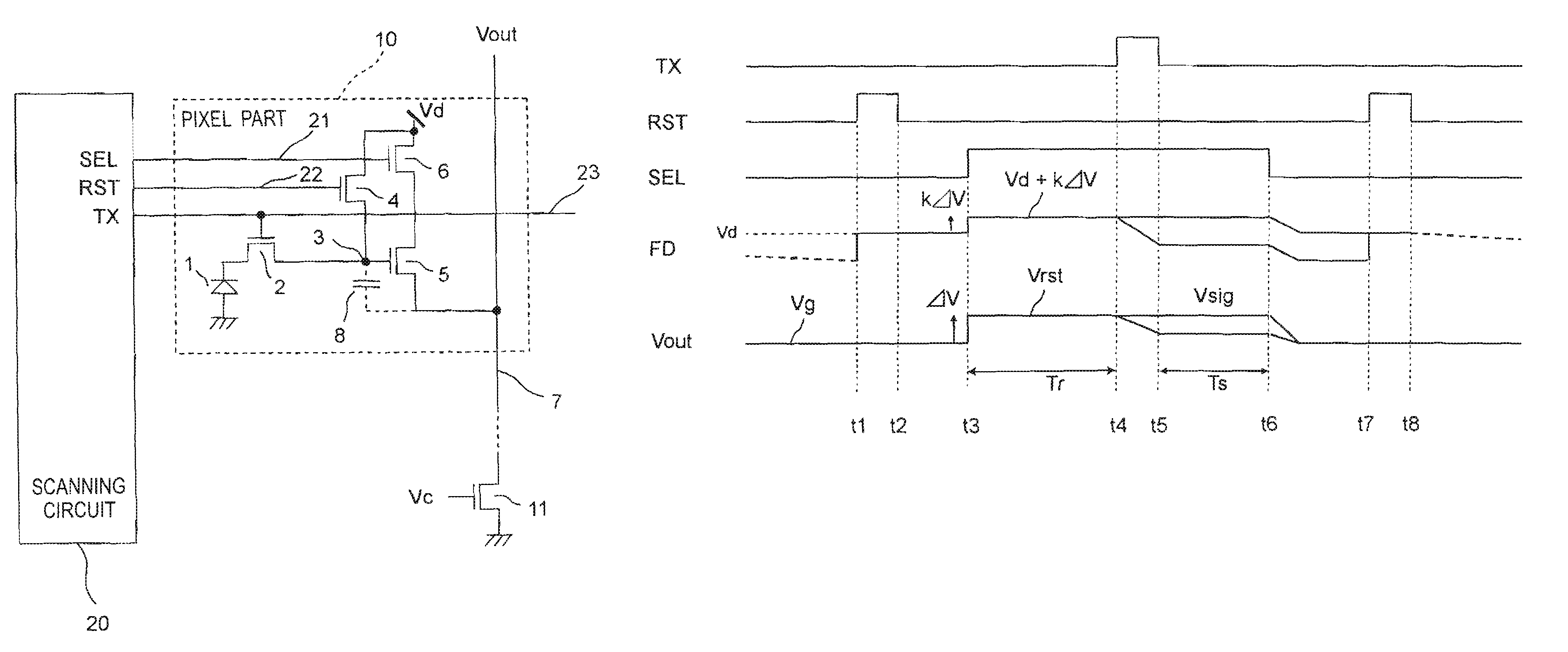
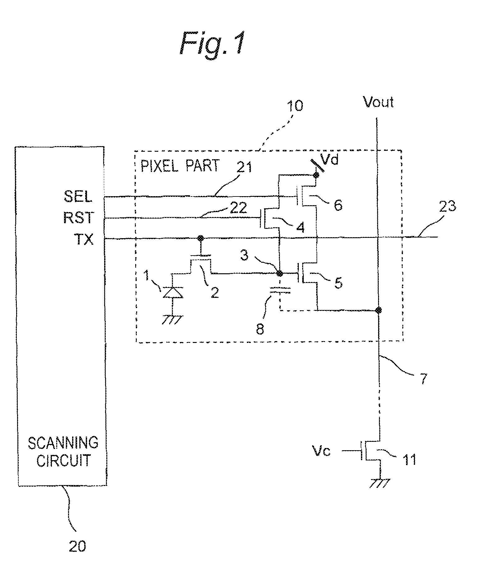
[0057]FIG. 1 is a circuit diagram showing the essential part of the amplification type solid-state imaging device of the first embodiment of the invention. The amplification type solid-state imaging device of the first embodiment has a plurality of pixel parts 10 arranged in a matrix form and a scanning circuit 20 as one example of the control section to control the pixel parts 10. In FIG. 1, only one pixel part 10 is shown. The pixel part 10 and the scanning circuit 20 are formed on a semiconductor substrate (not shown).

[0058]The pixel part 10 has an embedded type photodiode 1 as one example of the photoelectric transducer, a transfer transistor 2 that transfers a signal charge from the photodiode 1, a signal charge accumulating portion 3 that accumulates the signal charge of the photodiode 1 transferred from the transfer transistor 2, a reset transistor 4 that resets the voltage of the signal charge accumulating portion 3, an amplifying transistor 5 that am...

second embodiment

[0080](Second Embodiment)

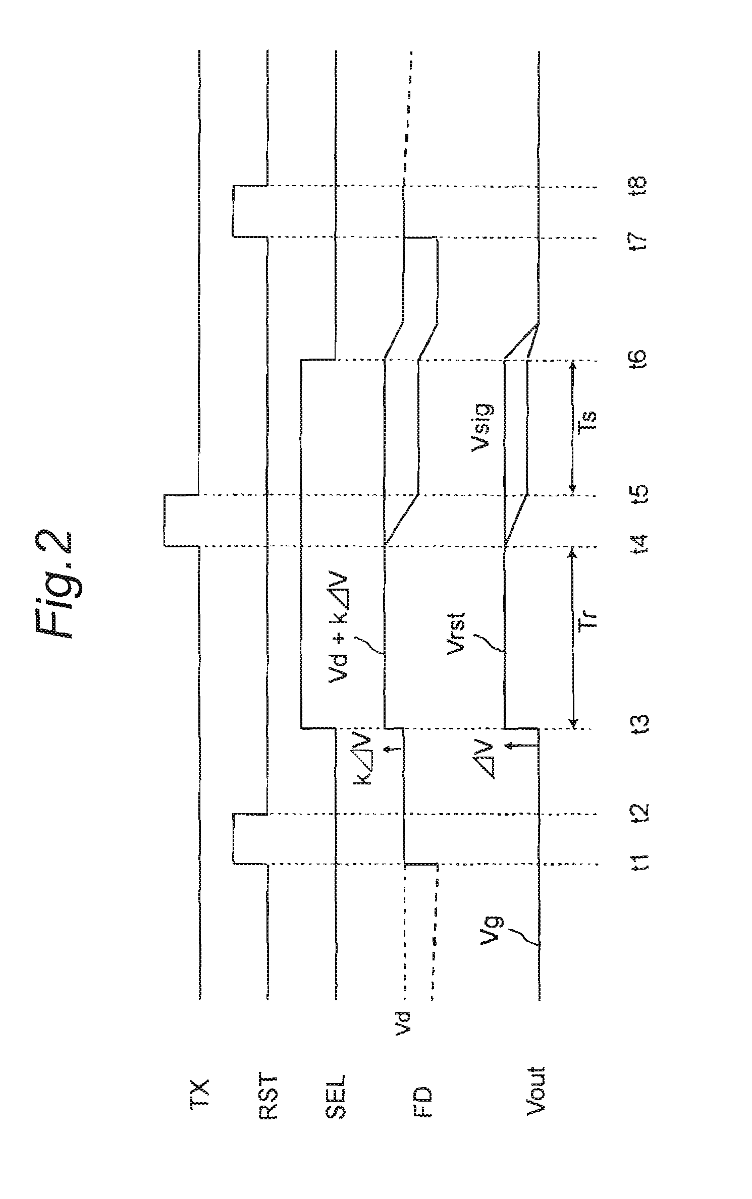
[0081]FIG. 3 is a timing chart showing the essential part of an amplification type solid-state imaging device according to a second embodiment of the invention. In this case, the circuit diagram of the objective pixel part is the same as that of the pixel part of the amplification type solid-state imaging device of the first embodiment shown in FIG. 1.

[0082]The amplification type solid-state imaging device of the second embodiment has a timing different from the timing chart shown in FIG. 2 of the first embodiment in the point that the reset signal RST is fixed to high level until time t2 and after time t7, i.e., the point that the low level is only in the period of t2 to t7. In FIG. 3, the period of t1 to t8 is that same as in FIG. 2, and therefore, the operation in the period is the same as in FIG. 2. Further, in the case of FIG. 3, the reset transistor 4 is consistently on until time t1 and after time t8 in a non-read period, and therefore, the voltage of...

third embodiment

[0083](Third Embodiment)

[0084]FIG. 4 is a circuit diagram showing the essential part of an amplification type solid-state imaging device according to the third embodiment of the invention. The amplification type solid-state imaging device of the third embodiment has the same construction as that of the amplification type solid-state imaging device of the first embodiment except that the reset transistor 14 and the select transistor 16 are depletion type MOS type transistors, a switch transistor 12 is provided between the read signal line 7 and the constant current load 11 and except a scanning circuit 40.

[0085]As shown in FIG. 4, the amplification type solid-state imaging device of the third embodiment has a plurality of pixel parts 30 arranged in a matrix form and the scanning circuit 40 as one example of the control section to control the pixel parts 30. In FIG. 4, only one pixel part 30 is shown. The pixel parts 30 and the scanning circuit 40 are formed on a semiconductor substra...


PUM


Abstract

Before a signal charge from a photodiode 1 is transferred to a signal charge accumulating portion 3 by a scanning circuit 20, a reset transistor 4 is turned on for a prescribed period to reset the voltage of the signal charge accumulating portion 3 in a state in which the voltage of a read signal line 7 is retained at a first voltage (Vg) by lowering the drain side voltage of an amplifying transistor 5. Subsequently, by raising the drain side voltage of the amplifying transistor 5 by a scanning circuit 20 to make the read signal line 7 have a second voltage (Vrst) higher than the first voltage (Vg), the voltage of the signal charge accumulating portion 3 is made higher than a voltage immediately after resetting. Then, the transfer transistor 2 is turned on to transfer the signal charge from the photodiode 1 to the signal charge accumulating portion 3.

Description

TECHNICAL FIELD[0001]The present invention relates to amplification type solid-state imaging devices having an amplifier circuit in its pixel part and more particularly to an improvement in the performance of the amplification type solid-state imaging device.BACKGROUND ART[0002]In general, a popularized amplification type solid-state imaging device has a pixel part having an amplification function and a scanning circuit placed in the periphery of the pixel part, where data are read from the pixel part by the scanning circuit.[0003]As one example of the amplification type solid-state imaging device, an APS (Active Pixel Sensor) type image sensor in which the pixel part is constructed of CMOS (complementary metal oxide semiconductor) advantageous for integration of the pixel part with a peripheral driving circuit and a signal processing circuit is known. Among the APS type image sensors, a four-transistor type capable of obtaining a high image quality is becoming mainstream in recent ...

Claims


Application Information

Patent Timeline
Patent Type & Authority Patents(United States)
IPC IPC(8): H04N3/14H04N5/335H01L27/00H01L27/146H04N5/357H04N5/369H04N5/374H04N5/3745H04N5/376
CPCH04N5/3597H04N5/37452H04N25/626H04N25/771
Inventor WATANABE, TAKASHIYOSHIMOTO, TAKAHIKO
Owner SHARP KK
Why Eureka
Try Eureka