Bottom gate type thin film transistor, method of manufacturing the same, and display apparatus

a thin film transistor and bottom gate technology, applied in the direction of transistors, electroluminescent light sources, electric lighting sources, etc., can solve the problems of high etching speed, difficult to produce a large-area tft with high yield, and damage to the oxide semiconductor layer, etc., to achieve the effect of achieving mass production

Inactive Publication Date: 2012-04-03
CANON KK
View PDF25 Cites 260 Cited by
  • Summary
  • Abstract
  • Description
  • Claims
  • Application Information

AI Technical Summary

Benefits of technology

[0018]Accordingly, it is an object of the present invention to attain formations of a source electrode and a drain electrode by etching in a bottom gate type thin film transistor that uses an oxide semiconductor, to thereby attain a process that excels in mass production.
[0022]According to the present invention, the source electrode and a drain electrode can be formed by etching, which makes it possible to provide thin film transistors which are excellent in mass productivity and have such transistor characteristics has to have a minimized OFF-current.

Problems solved by technology

In lift-off, a problem arises such as readherence of particles of a lifted-off electrode film, thus it is difficult to produce a large-area TFT with high yields.
It is difficult to form a source electrode and a drain electrode by wet etching using an acid in designing a TFT, because even if an electrode material is a metal or a transparent oxide conductor, an oxide semiconductor whose main component is ZnO is susceptible to an acid and the etching speed is high.
However, in an oxide semiconductor whose main component is ZnO, an oxygen vacancy is liable to occur and many carrier electrons are liable to be generated, thus an oxide semiconductor layer may be damaged in a process of etching a source electrode and a drain electrode.
There is also a method of providing a protective layer as an etching stopper layer in order to decrease damage to the semiconductor layer caused by the etching, but, even if such a protective film is formed, the oxide semiconductor layer is damaged and an OFF-current becomes larger.
Thus, there is a problem in that TFT characteristics with a satisfactory on / off ratio are difficult to realize with stability.

Method used


Image

  • Bottom gate type thin film transistor, method of manufacturing the same, and display apparatus
  • Bottom gate type thin film transistor, method of manufacturing the same, and display apparatus
  • Bottom gate type thin film transistor, method of manufacturing the same, and display apparatus

Examples


example 1

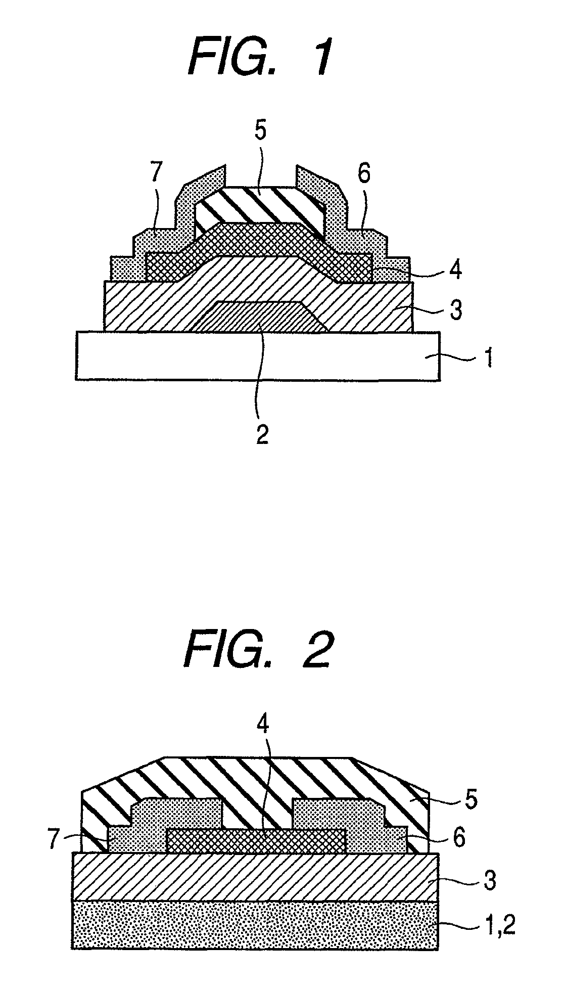
[0141]In this example, an inverted stagger (bottom gate) type MISFET device illustrated in FIG. 11 is produced.

[0142]First, a gate terminal of Ti of 5 nm / Au of 40 nm / Ti of 5 nm is formed on a glass substrate by photolithography and a lift-off technique.

[0143]Further, an insulating layer of a-SiOx with a thickness of 200 nm is formed thereon by sputtering. In this case, a SiO2 target is used as the sputtering target, and Ar gas is used as the sputtering gas. Also the RF radio-frequency power is 400 W, the deposition pressure is 0.1 Pa, and the film deposition rate is 7.4 nm / min. The substrate temperature is room temperature, and no intentional heating is performed.

[0144]Further, an amorphous oxide semiconductor film used as a semiconductor layer is formed thereon at room temperature with a thickness of 20 nm by an RF sputtering.

[0145]A channel region is formed by photolithography and wet etching using hydrochloric acid.

[0146]After that, Ti of 5 nm / Au of 40 nm / Ti of 5 nm is formed by ...

example 2

[0160]In this example, an inverted stagger (bottom gate) type MISFET device illustrated in FIG. 1 is produced.

[0161]First, a gate electrode layer of a transparent conductive film IZO with a thickness of 150 nm is formed on a glass substrate by sputtering.

[0162]A gate electrode is formed by photolithography and wet etching using hydrochloric acid.

[0163]Further, an insulating layer of a-SiOx with a thickness of 200 nm is formed thereon by an RF sputtering. In this case, a SiO2 target is used as the sputtering target, and Ar gas is used as the sputtering gas. Also the RF radio-frequency power is 400 W, the deposition pressure is 0.1 Pa, and the film deposition rate is 7.4 nm / min. The substrate temperature is room temperature, and no intentional heating is performed.

[0164]Further, an amorphous oxide semiconductor film used as a semiconductor layer is formed at room temperature with a thickness of 20 nm by sputtering.

[0165]A channel region is formed by photolithography and wet etching us...

example 3

[0172]In this example, a display apparatus using the TFT illustrated in FIG. 7 is described.

[0173]The production process of the TFT is similar to that of Example 3.

[0174]In the above-described TFT, a short side of an ITO film forming a drain electrode is extended to 100 μm. With 90 μm of the extended portion being left and with wiring to the source electrode and the gate electrode being secured, the TFT is covered with an insulating layer.

[0175]A polyimide film is applied thereon and rubbing is carried out.

[0176]On the other hand, a plastic substrate having an ITO film and a polyimide film similarly formed thereon with rubbing carried out is prepared, the plastic substrate is opposed to the above-described substrate having the TFT formed thereon with a gap of 5 μm therebetween, and nematic liquid crystal is injected into the gap.

[0177]Further, a pair of polarizing plates is provided on both sides of the structure.

[0178]In this case, by applying voltage to the source electrode of the...


PUM


Abstract

Provided is a bottom gate type thin film transistor including on a substrate (1) a gate electrode (2), a first insulating film (3) as a gate insulating film, an oxide semiconductor layer (4) as a channel layer, a second insulating film (5) as a protective layer, a source electrode (6), and a drain electrode (7), in which the oxide semiconductor layer (4) includes an oxide including at least one selected from the group consisting of In, Zn, and Sn, and the second insulating film (5) includes an amorphous oxide insulator formed so as to be in contact with the oxide semiconductor layer (4) and contains therein 3.8×10¹⁹ molecules / cm3 or more of a desorbed gas observed as oxygen by temperature programmed desorption mass spectrometry.

Description

TECHNICAL FIELD[0001]The present invention relates to a bottom gate type thin film transistor, a method of manufacturing the same, and an electro-optical apparatus such as a display apparatus. More particularly, the present invention relates to a bottom gate type thin film transistor provided with an insulating film as an etching stopper, a method of manufacturing the same, and a display apparatus.BACKGROUND ART[0002]In recent years, a thin film transistor (TFT) in which a transparent conductive oxide polycrystalline thin film containing ZnO as a main ingredient is used as a channel layer has been actively developed (see Japanese Patent Application Laid-Open No. 2002-76356 and U.S. Publication No. 2006 / 0244107 A1).[0003]The thin film can be formed at low temperature and is transparent to visible light, so it is possible to form a flexible transparent TFT on a substrate such as a plastic plate or a film.[0004]Further, it is disclosed that thin film transistors having a transparent se...

Claims


Application Information

Patent Timeline
Patent Type & Authority Patents(United States)
IPC IPC(8): H01L33/00H01L29/786H01L21/336H05B44/00
CPCH01L29/7869H01L27/1225H01L29/66969H01L29/78606
Inventor HAYASHI, RYOKAJI, NOBUYUKIYABUTA, HISATO
Owner CANON KK
Why Eureka
Try Eureka