Plasma processing method

a processing method and plasma technology, applied in the field of plasma processing methods, can solve the problems of limited effective range, reaction product cannot be fully removed from a portion, and limit the effective range of plasma processing apparatus capable, so as to suppress the flaking of reaction product and achieve the effect of achieving mass production consistency

Inactive Publication Date: 2011-05-12
HITACHI HIGH-TECH CORP
View PDF7 Cites 2 Cited by
  • Summary
  • Abstract
  • Description
  • Claims
  • Application Information

AI Technical Summary

Benefits of technology

The use of the above-described configuration makes it possible to provide a plasma processing method that excels in mass production consistency as it suppresses the

Problems solved by technology

As described above, a limit is imposed on the effective range of the plasma processing apparatus that is capable of cleaning the inner wall of the vacuum vessel or reducing the amount of reaction product deposition on the inner wall of the vacuum vessel when a high-frequency power supply is connected to the Faraday field between the inductive antenna and plasma to supply electrical power.
The effective range is limited because the plasma processing apparatus merely works on a portion that is formed with a

Method used


Image

  • Plasma processing method
  • Plasma processing method
  • Plasma processing method

Examples


first embodiment

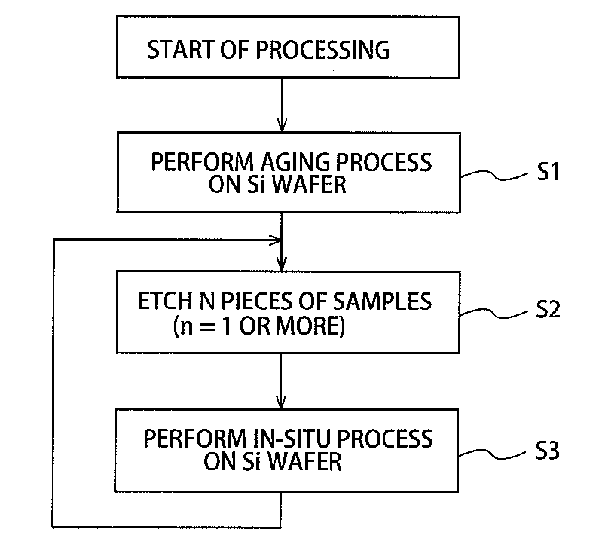
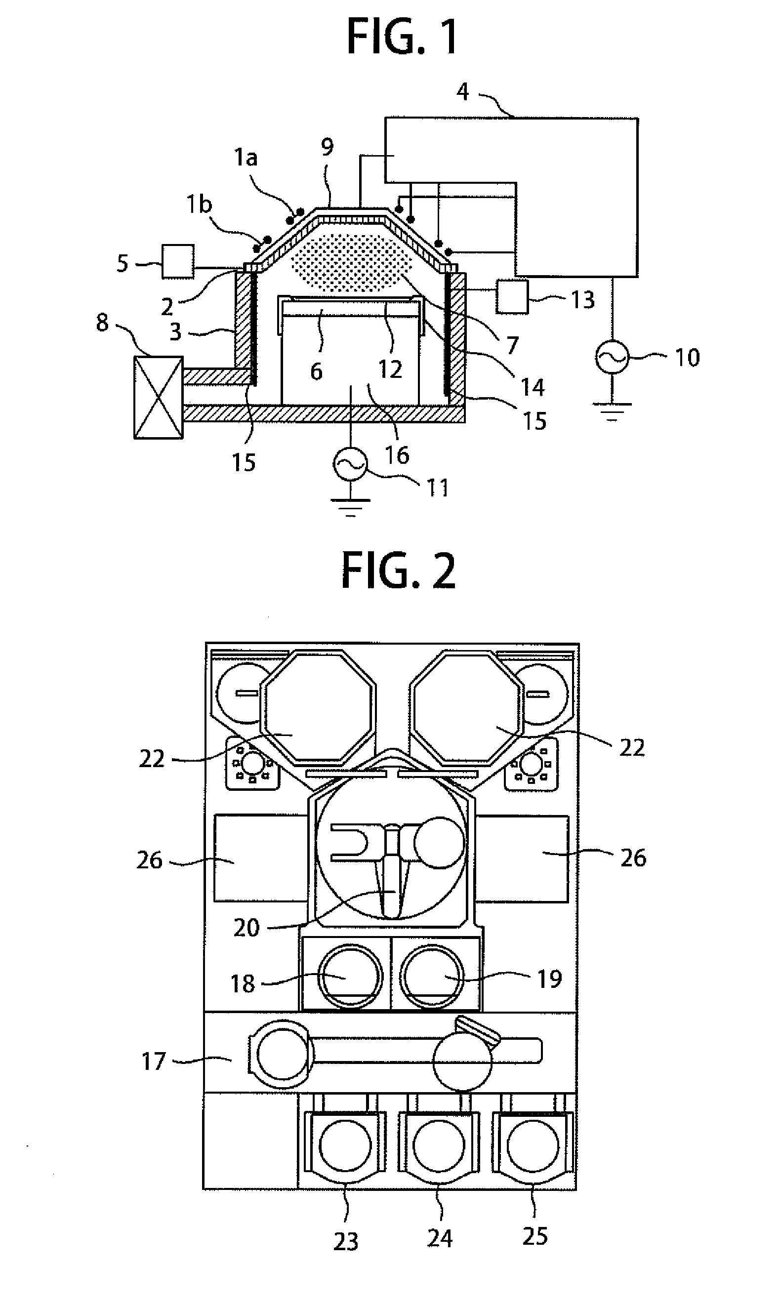
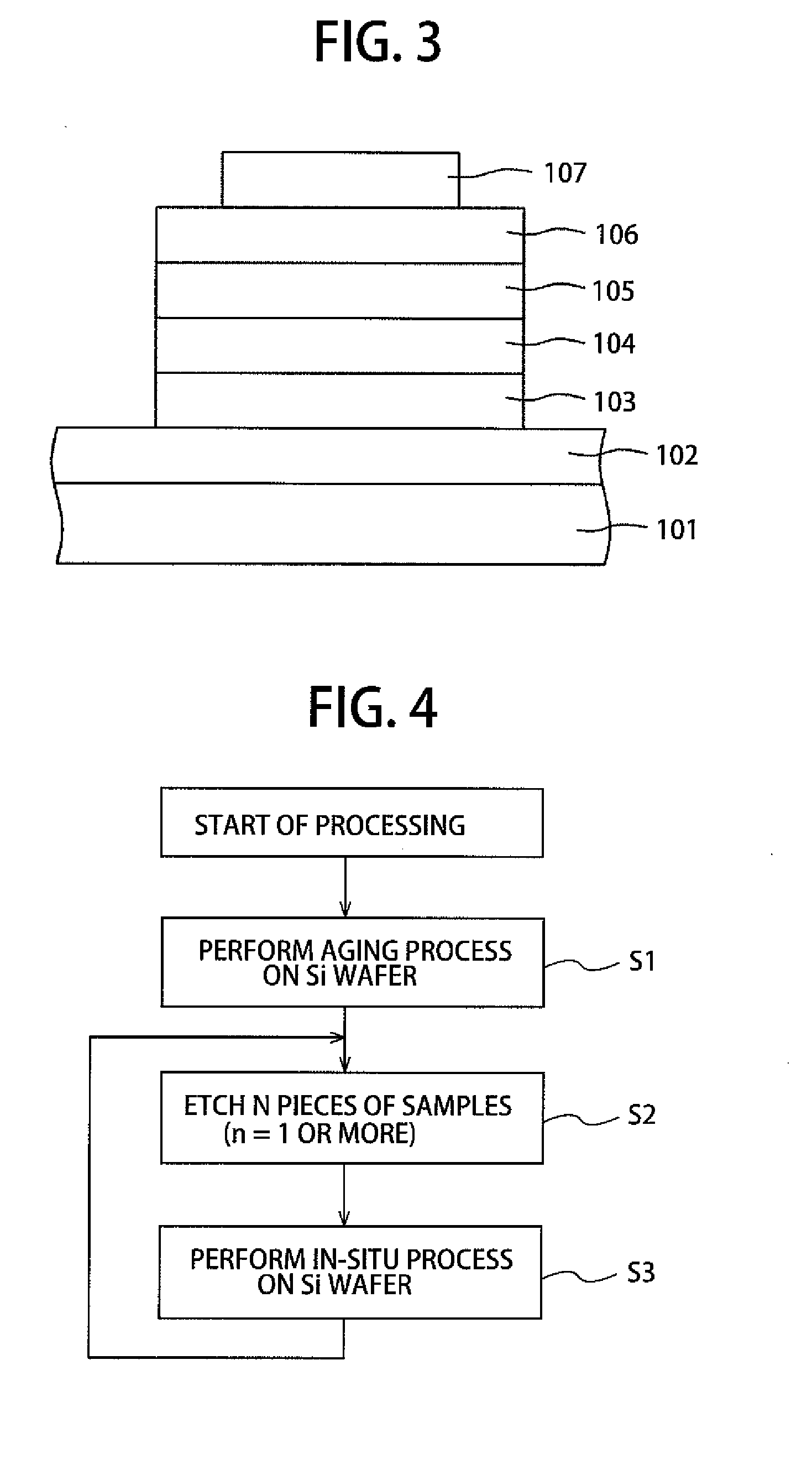
A first embodiment of the present invention will now be described with reference to FIGS. 1 to 5,6A and 6B. FIG. 1 is a schematic cross-sectional view illustrating a vacuum processing apparatus according to the first embodiment. The present embodiment assumes that a plasma etching apparatus is used as the vacuum processing apparatus.

The plasma etching apparatus is a processing apparatus for etching various thin films formed on a semiconductor substrate. It receives the supply of a plasma formation gas, generates plasma, and etches a metallic film or other thin film formed on the substrate.

In the plasma processing apparatus shown in FIG. 1, a processing room, which is enclosed by a bell jar and a chamber, includes a discharger 2, which is covered with the bell jar and made of a nonconductive ceramic material to form a plasma generation section; and a processor 3, which is enclosed by the chamber and provided with a sample 12 to be processed and an electrode 6 for high-frequency bias ...

second embodiment

A second embodiment of the present invention will now be described. However, the differences between the second embodiment and the first embodiment, which has been described above, will be mainly described while skipping the description of matters common to these two embodiments.

The second embodiment will be described with reference to a case where the inner wall of the chamber is heated before aging. As regards the hardware configuration, the second embodiment assumes that a heater is mounted on the outer circumference of the processor (chamber) 3 of the etching apparatus shown in FIG. 1. The etching apparatus was used to etch a sample by performing the steps shown in FIG. 4. The second embodiment differs from the first embodiment in that the processor 3 is heated by the heater (thermal aging) before the aging process on the Si wafer (step S1). The second embodiment assumes that the heater is set to a heating temperature of 100° C. However, the heating temperature setting is variab...


PUM


Abstract

Disclosed is a plasma processing method that excels in mass production consistency as it suppresses the flaking of a reaction product deposited on a portion outside the effective range of a Faraday shield in a vacuum vessel. The plasma processing method, which plasma-processes a sample having a layer made of an etch-resistant material by using a plasma processing apparatus having a discharger and a processor, includes a first step of performing an aging process that is to be performed before etching the sample, a second step of performing etching by plasma-processing the layer that is made of an etch-resistant material and formed on the sample, a third step of stabilizing a film deposited on the inner wall of a chamber forming the processor by performing plasma processing after the second step, and an additional step of repeating the second step and the third step.

Description

CLAIM OF PRIORITYThe present application claims priority from Japanese Patent Application JP 2009-254855 filed on Nov. 6, 2009, the content of which is hereby incorporated by reference into this application.BACKGROUND OF THE INVENTION(1) Field of the InventionThe present invention relates to a plasma processing method, and more particularly to a plasma processing method suitable for etching an etch-resistant material in a vacuum processing vessel.(2) Description of the Related ArtIn recent years, materials to be etched in the field of manufacturing semiconductor devices such as a DRAM (Dynamic Random Access Memory) and a logic circuit IC are relatively etch-resistant materials such as Si, Al, and SiO2. Further, Fe and other similar etch-resistant materials are used for FRAMs (Ferroelectric Random Access Memories), MRAMs (Magnetoresistive Random Access Memories), magnetic heads, and the like.More specifically, the etch-resistant materials include Fe, NiFe, PtMn, and IrMn, which are f...

Claims


Application Information

Patent Timeline
IPC IPC(8): H01L21/3065
CPCH01J37/321H01L21/32136H01L21/31122
Inventor SUYAMA, MAKOTOSHIMADA, TAKESHIYOSHIDA, ATSUSHIMORIOKA, YASUKIYOTANAKA, KOTA
Owner HITACHI HIGH-TECH CORP
Why Eureka
Try Eureka