Timer for low-power and high-resolution with low bits derived from set of phase shifted clock signals

a clock signal and low-power technology, applied in the direction of generating/distributing signals, instruments, pulse techniques, etc., can solve the problems of limiting the resolution of the timer and the overall performance of the timer, increasing the power consumption of digital circuitry, and increasing the clock frequency. achieve the effect of a favorable ratio

Active Publication Date: 2012-05-22
TEXAS INSTR INC
View PDF9 Cites 4 Cited by
  • Summary
  • Abstract
  • Description
  • Claims
  • Application Information

AI Technical Summary

Benefits of technology

[0004]It is an object of the present invention to provide a timer, which gives the same resolution of time and performance as a conventional timer, with a reduced clock frequency and power consumption.
[0014]Furthermore, the electronic device may either store the timer value when the complete timer value or the states of the m delayed signals are output from the first counter stage. Since converting the m delayed signals into the timer value may constitute the most critical path, it is advantageous to store the states of the m delayed clock signals between the output of the first counter stage and the input of the code converter stage.
[0019]According to another aspect of the present invention, an electronic device includes a pulse width modulator. The pulse width modulator includes a clock signal generating stage providing a first set of m phase shifted clock signals having m different phases, a decoding stage coupled to an output of the clock signal generating stage selecting one of the phase shifted clock signals to provide an edge of a pulse of the pulse width modulated signal within a period of the clock signal. In an advantageous implementation, the clock generation stage includes a plurality of delay elements. Each delay element has a delay that is substantially smaller than a clock period of the clock signal used for the pulse width modulator. The delay elements are coupled in a chain, the first delay element in the chain receiving the clock signal as an input signal. This provides a set of phase shifted clock signals at the outputs of the delay elements. A decoding stage receives the outputs of the delay elements and selects one of the phase shifted clock signals to provide an edge of a pulse of the pulse width modulation signal within a period of the clock signal. According to this aspect of the present invention, the pulse width modulator benefits from the basic idea of the present invention. The pulse width modulator uses a set of phase shifted clock signals instead of a high basic clock frequency to achieve a high time resolution. The basic period of the clock signal is not prolonged by a specific delay, but rather is subdivided by the edges of a set of phase shifted clock signals of the same frequency into smaller periods of time. This achieves a resolution that is a factor m higher than in conventional circuits without increasing the circuit complexity or the power consumption.
[0020]The present invention is also a method of providing a binary timer value. Accordingly, clock cycles of a clock signal are counted in order to receive a count representing a plurality of most significant bit values of the binary timer value. A set of phase shifted clock signals is generated. Each of the phase shifted clock signals is delayed with respect to another clock signal by less than a clock period of the clock signal. A plurality of least significant bit values based on the states of the phase shifted clock signals of the set of phase shifted clock signals at a point of time of an event is determined. The binary timer value includes the least significant bit values and the most significant bit values. Thus the binary timer value consists partially of the least significant bit values and the most significant bit values. The method according to the present invention saves a considerable amount of power because the clock frequency can be substantially smaller than with a conventional system.
[0022]According to an advantageous aspect of the present invention, a delay element can provide a delay of tT. The delay tT can be 2(−k) / fIN, with k being an integer number greater than 0 and fIN being the frequency of the input clock signal of the chain of delay elements. Generally, tT can be any fraction 1 / fIN, but a binary ratio can be advantageous in many applications. In particular, if the number m of delayed clock signals is chosen equal to 2k, which means that k=n with n as previously defined, a very advantageous ratio can be achieved.

Problems solved by technology

Power consumption of digital circuitry increases with increasing clock frequency.
This limits the resolution of the timer and the overall performance of the timer.

Method used


Image

  • Timer for low-power and high-resolution with low bits derived from set of phase shifted clock signals
  • Timer for low-power and high-resolution with low bits derived from set of phase shifted clock signals
  • Timer for low-power and high-resolution with low bits derived from set of phase shifted clock signals

Examples


Embodiment Construction

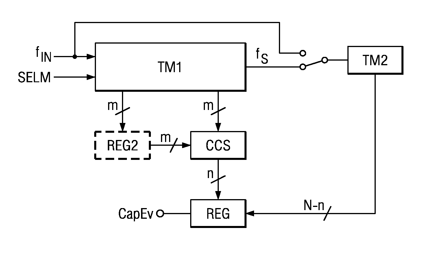
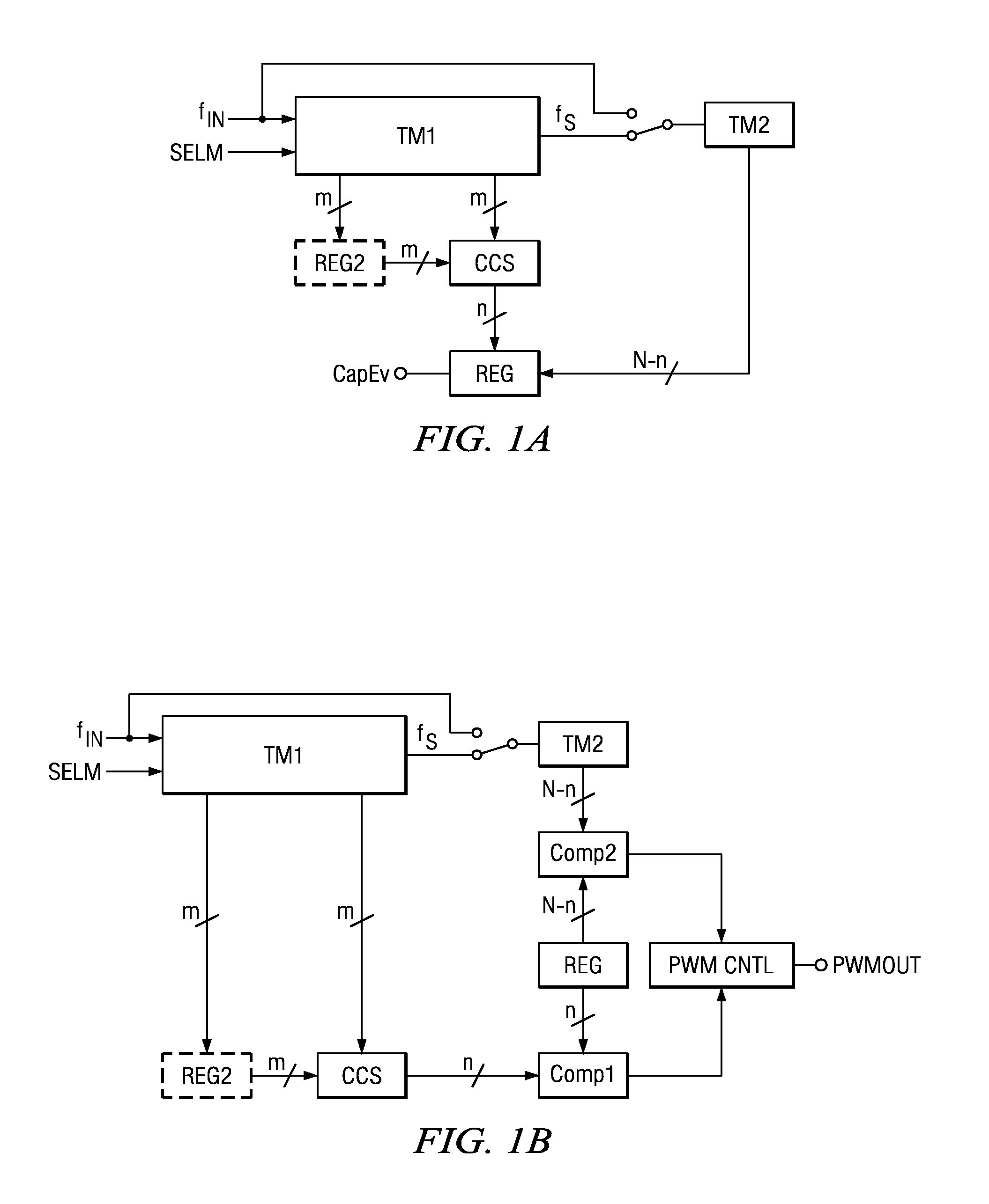
[0031]FIG. 1A shows a simplified block diagram of a first embodiment of the present invention which has an input capture mode. The electronic device includes a first counter stage TM1 and a second counter stage TM2. Both counter stages receive the input clock signal fIN as an input clock signal. The second counter stage TM2 includes a conventional counter which typically includes a chain of storing units such as flip-flops. First counter stage TM1 includes a chain of delay elements (i.e. a ring oscillator) and outputs a set of m phase shifted clock signals to code converter stage CCS. Capture event signal CapEv issues upon occurrence of a specific event. Select timer value signal SELM prompts first counter stage TM1 to output the states of the set of m phase shifted clock signals to code converter stage CCS. Code converter stage CCS converts the states of the set of m phase shifted clock signals into a group of n least significant bits of a count value of bit length n. The number of...


PUM


Abstract

The present invention is an electronic device comprising a counter driven by an input clock signal for counting clock cycles and providing most significant bits of a count. A clock signal generating stage provides a first set of phase shifted clock signals having m different phases. The electronic device determines n least significant bits of the count of the counter from the logic states of the first set of m phase shifted clock signals.

Description

CLAIM OF PRIORITY[0001]This application claims priority under 35 U.S.C. 119(a) to German Patent Application No. 10 2008 023 536.9 filed May 14, 2008 and under 35 U.S.C. 119(e) (1) to U.S. Provisional Application No. 61 / 141,896 filed Dec. 31, 2008.TECHNICAL FIELD OF THE INVENTION[0002]The technical field of this invention is an electronic device comprising circuitry for timing signals.BACKGROUND OF THE INVENTION[0003]Power consumption of digital circuitry increases with increasing clock frequency. It is desirable to reduce the clock frequency of a clock used for digital signal processing. Sophisticated electronic components require ever higher data throughput and therefore higher clock frequencies. The highest clock frequency in a system determines the highest possible resolution in time. A timer includes a counter, which is typically a chain of flip-flops that is driven by the system clock. The output of each flip-flop represents a single bit of a binary count representing the timer...

Claims


Application Information

Patent Timeline
Patent Type & Authority Patents(United States)
IPC IPC(8): G06F1/04
CPCH03K5/1504H03M1/822H03K2005/00286
Inventor DIEWALD, HORSTSCHREINER, JOERG
Owner TEXAS INSTR INC
Why Eureka
Try Eureka