Semiconductor sensor and method of manufacturing the same

a technology of semiconductors and sensors, applied in the field of semiconductor sensors, can solve the problems of extending cracking, distorted diaphragms to have temperature characteristics, and distorted diaphragms, and achieves the effects of high etching selectivity, short manufacturing time, and fast etching ra

Active Publication Date: 2012-05-29
ORMON CORP
View PDF12 Cites 9 Cited by
  • Summary
  • Abstract
  • Description
  • Claims
  • Application Information

AI Technical Summary

Benefits of technology

[0013]In a semiconductor sensor in accordance with one aspect of the present invention, the insulating layer is removed in most of the sensitive region (diaphragm) of the second semiconductor layer. This reduces temperature characteristics in the semiconductor sensor because of a difference in coefficient of thermal expansion between the sensitive region and the insulating layer, which occur in cases where an entire bottom surface of the sensitive region is covered with an insulating layer. Further, cracking never expands from the insulating layer to the sensitive region.
[0014]Furthermore, since an outer circumference of the sensitive region of the second semiconductor layer is covered with the insulating layer slightly remaining on the bottom surface of the sensitive region and is reinforced by the insulating layer, the sensitive region becomes resistant to breakage even if the sensitive region is repeatedly deformed. Thus, in accordance with one aspect of the invention, the sensitive region of the second semiconductor layer becomes resistant to breakage. In addition, since the film thickness of the sensitive region need not be decreased by digging down the bottom surface of the sensitive region, the possibility of variations in sensitivity of the semiconductor sensor is reduced.
[0015]According to the semiconductor sensor of another embodiment of the present invention, the sensitive region has a film thickness equal to a film thickness of a region other than the sensitive region of the second semiconductor layer. In accordance with this embodiment, since the sensitive region of the second semiconductor layer is not made thinner than a region other than the sensitive region by etching, the possibility of variations in sensitivity of the semiconductor sensor because of variations in film thickness of the sensitive region is reduced. Further, a bottom surface of the second semiconductor layer is flat. This reduces stress concentration due to a corner, making the sensitive region resistant to breakage.
[0016]According to the semiconductor sensor of another embodiment of the present invention, in the insulating layer covering the second semiconductor layer in the outer circumference of the top surface of the recess, a film thickness becomes thinner from an outer circumference side of the sensitive region toward a center of the sensitive region. In accordance with this embodiment, the insulating layer covering the outer circumference of the sensitive region becomes gradually thinner toward the tip. This makes it difficult for deformation of the sensitive region to be inhibited by the insulating layer.
[0018]In accordance with a method of manufacturing the semiconductor sensor in accordance with one aspect of the invention, a semiconductor sensor having effects as mentioned above can be manufactured. Further, at the time of etching the insulating layer, the insulating layer is etched up to the midpoint at a relatively fast etching rate by dry etching, and subsequently the remaining insulating layer is removed by etching with a relatively high etching selectivity. This makes it possible to expose the second semiconductor layer from the insulating layer, in the top central portion in the recess, in a relatively short manufacturing time, and to leave the insulating layer at a top outer circumference in the recess. Further, by adjusting a timing of changing from fast etching to slow etching, the shape and dimensions of the insulating layer remaining at the outer circumference of the sensitive region can be adjusted.

Problems solved by technology

However, in such a pressure sensor, the diaphragm is distorted to have temperature characteristics because of a difference in coefficient of thermal expansion between the insulating layer and the Si thin film layer.
The deformation of the diaphragm causes cracking to occur in the insulating layer.
There is therefore a possibility that cracking extends to the Si thin film layer to break the diaphragm.
No matter how accurate the time management is, however, various variable factors in a process of etching a diaphragm cannot be avoided.
The variable factors lead to variations in depth of a depression, making it difficult to uniform the thickness of a diaphragm.
There has been a possibility that the diaphragm is broken from the corner.
This reduces temperature characteristics in the semiconductor sensor because of a difference in coefficient of thermal expansion between the sensitive region and the insulating layer, which occur in cases where an entire bottom surface of the sensitive region is covered with an insulating layer.
This makes it difficult for deformation of the sensitive region to be inhibited by the insulating layer.

Method used


Image

  • Semiconductor sensor and method of manufacturing the same
  • Semiconductor sensor and method of manufacturing the same
  • Semiconductor sensor and method of manufacturing the same

Examples


first embodiment

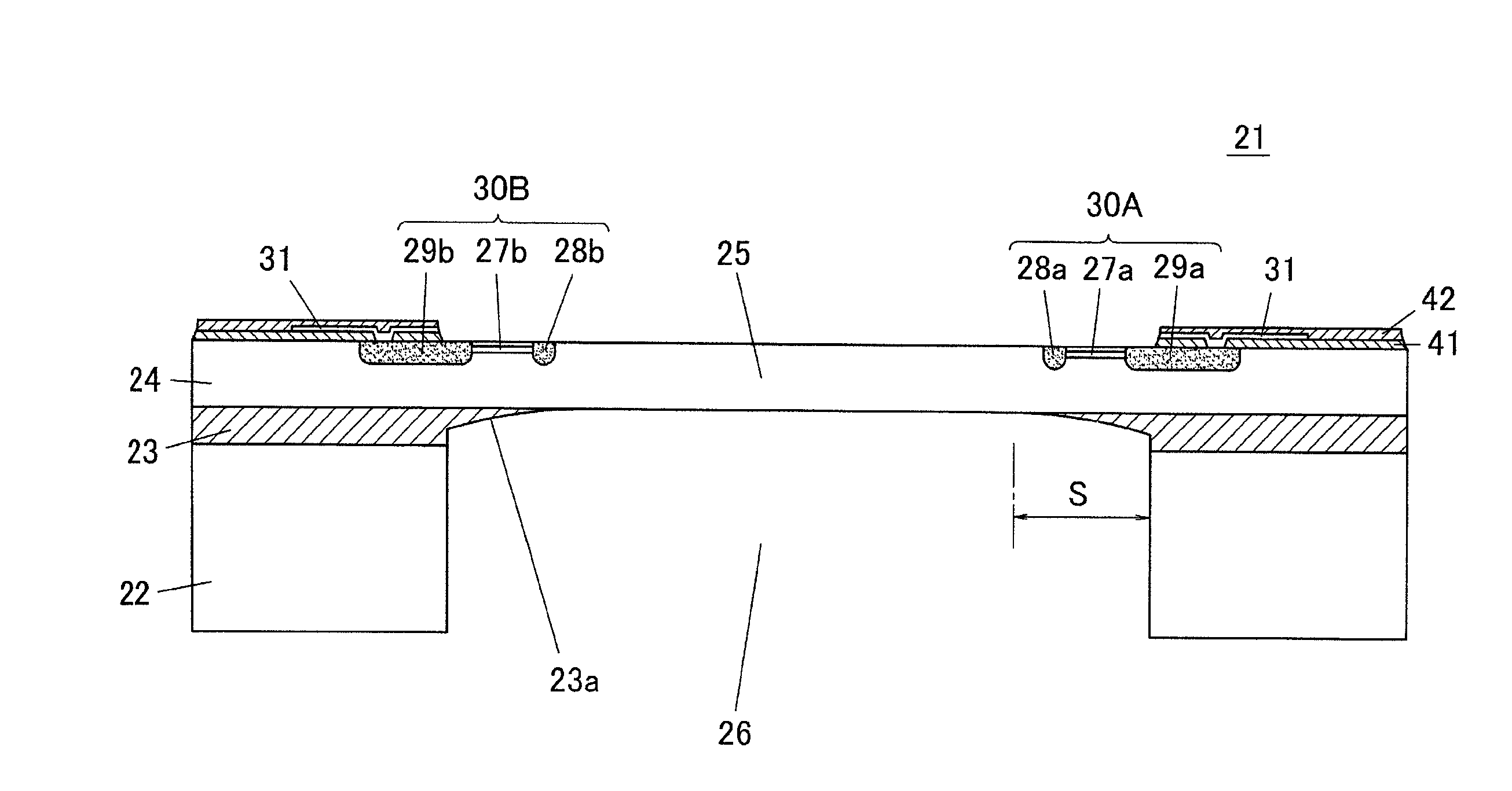
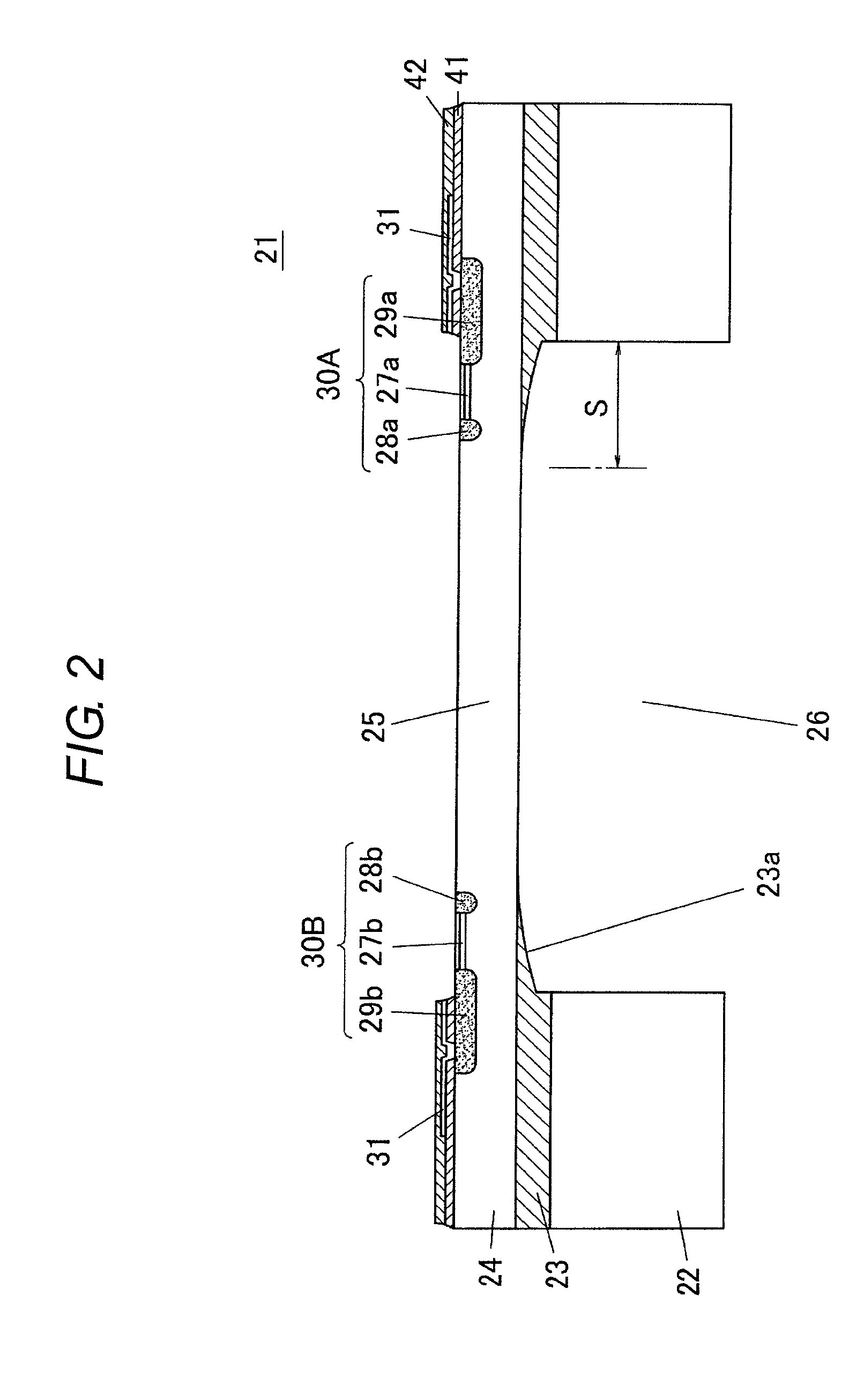
[0027]FIG. 2 is a sectional view showing a semiconductor sensor according to a first embodiment of the invention, that is, a pressure sensor 21. With reference to FIG. 2, the structure of the pressure sensor 21 is described. As shown in FIG. 2, the pressure sensor 21 is manufactured using an SOI substrate. An SOI substrate is obtained by bonding an N-type Si substrate 22 (first semiconductor layer) and an N-type Si thin film 24 (second semiconductor layer) with a SiO2 film 23 (insulating layer) interposed therebetween. The pressure sensor 21 has a round diaphragm 25 (sensitive region that is not fixed to the Si substrate 22) formed of part of the Si thin film 24. The diaphragm 25 is slightly displaced in the film direction by a pressure of an object being sensed.

[0028]The pressure sensor 21 has a cylindrical recess 26 (cavity) formed from a bottom surface of the Si substrate 22 up to a top surface of the SiO2 film 23, in accordance with a bottom surface of the diaphragm 25. In a top...

second embodiment

[0051]FIG. 6 is a cross-sectional view showing a pressure sensor 51 according to a second embodiment of the invention. In this embodiment, the recess 26 has a tapered top such that the horizontal cross-sectional area of the recess 26 increases from the top toward the bottom.

[0052]FIGS. 7A to 7D are cross-sectional views showing a method of manufacturing the pressure sensor 51 of the second embodiment. FIG. 7A shows the same SOI substrate as that in FIG. 3B described in the manufacturing method of the first embodiment. The resist 44 is formed on the bottom surface of the Si substrate 22, and the opening 45 is made in the resist 44. However, a material resistant to an etchant used in a wet etching process, such as TMAH and KOH, is used as the resist 44.

[0053]Subsequently, anisotropic etching of the Si substrate 22 is performed through the opening 45 of the resist 44 by a wet etching process, digging down the recess 26 in a tapered shape. The etching is performed until the bottom surfa...


PUM


Abstract

A semiconductor sensor has a first semiconductor layer as a base, an insulating layer formed on the first semiconductor layer, and a second semiconductor layer formed on the insulating layer. A recess is formed from a bottom surface of the first semiconductor layer up to a top surface of the insulating layer. The second semiconductor layer is covered with the insulating layer in an outer circumference of a top surface of the recess. A sensitive region of the second semiconductor layer is exposed in a region except the outer circumference of the top surface of the recess.

Description

BACKGROUND OF THE INVENTION[0001]1. Technical Field[0002]The present invention relates to a semiconductor sensor with a diaphragm (a sensitive region of a semiconductor thin film) and a method of manufacturing the semiconductor sensor.[0003]2. Related Art[0004]Small-sized pressure sensors, vibration sensors and the like using semiconductor substrates have diaphragms for detecting pressures and vibrations. Methods of manufacturing diaphragms in semiconductor substrates include a method using a silicon on insulator (SOI) wafer in which a Si substrate and a thin film layer are bonded with an insulating layer interposed therebetween as disclosed in Japanese Patent No. 3506932 and Japanese Unexamined Patent Publication No. 2002-208708.[0005]For example, in a semiconductor pressure sensor disclosed in Japanese Patent No. 3506932, which is shown in FIG. 1, an SOI wafer in which an insulating layer 12 (SiO2 layer) and a Si thin film layer 13 (Si layer) are laminated on a Si substrate 11 (Si...

Claims


Application Information

Patent Timeline
Patent Type & Authority Patents(United States)
IPC IPC(8): H01L29/84
CPCG01L9/0042G01L9/0054G01L9/0048B81B3/007B81B2201/0264B81B2203/0127
Inventor ADACHI, YOSHITAKAINOUE, KATSUYUKI
Owner ORMON CORP
Why Eureka
Try Eureka