Method for manufacturing thin film transistors

a technology of thin film transistors and manufacturing methods, applied in semiconductor devices, identification means, instruments, etc., can solve the problems of prone to cracking during manufacture, low heat resistance, and inability to use the current glass substrate line, so as to achieve the effect of reducing the cos

Active Publication Date: 2012-06-12
PANASONIC LIQUID CRYSTAL DISPLAY CO LTD +1
View PDF27 Cites 24 Cited by
  • Summary
  • Abstract
  • Description
  • Claims
  • Application Information

AI Technical Summary

Benefits of technology

[0008]The present invention intends to provide a method of forming TFT on a plastic substrate by a transfer method, not requiring to lower the process temperature, capable of using a current line and capable of decreasing the cost.
[0022]The present invention provides a method of forming TFT on a plastic substrate by a transfer method, having no requirement for lowering the process temperature, capable of using a current line, and decreasing the cost.

Problems solved by technology

However, use of a glass substrate at the thickness less than that described above results in a problem that it tends to be cracked during manufacture or during use.
However, while the heat resistance of the glass substrate is about 600° C., the plastic substrate has the heat resistance usually of about 200° C. and involves a problem that the heat resistance is low.
Further since the plastic substrate is soft and flexible different from the glass substrate, it involves a drawback that a line provided for current glass substrates cannot be used as it is.
While the method of once forming TFT on the glass substrate and then decreasing the thickness of the glass has an advantage capable of using the current line and using a current process temperature as it is, when an etching step is adopted for the step of reducing the thickness of the glass substrate, almost of the glass substrate is lost wastefully to result in a drawback of increasing the cost.
Further, the method of bonding the plastic substrate on the glass substrate, forming TFT thereon and then conducting separation involves a problem in view of the heat resistance of the plastic substrate and, accordingly, results in a drawback that the process temperature has to be lowered and a device of excellent characteristics cannot be obtained.

Method used


Image

  • Method for manufacturing thin film transistors
  • Method for manufacturing thin film transistors
  • Method for manufacturing thin film transistors

Examples


first example

Manufacture of Heat Resistant Transparent Polymer Film (a)

[0153]A solution of polybenzoxazole precursor (VIII) in propylene glycol monomethyl ether acetate (PGMEA) / γ-butylolactone (BLO) (1 / 9) was spin coated on a quartz support substrate of 0.6 mm thickness. Then, pre-baking was conducted at 120° C. for 3 min to obtain a coating film of 5.5 μm thickness.

[0154]

[0155]Then, after baking by using an inert gas oven under nitrogen at 200° C. for 30 min, cure baking was conducted at 350° C. for 1 hour to obtain a polybenzoxazole film (B-1) as the polymer film (a) of the invention. The thickness after curing was 4.8 μm. The layer after curing was colorless and transparent.

[0156]

[0157]FIG. 17 shows transmission spectra in a region at a wavelength of from 300 nm to 800 nm of a cured layer obtained as described above. It was found that this cured layer showed transmittance of about 90% or higher in a range from 400 nm to 800 nm as a visible region. Further, it was found that transmittance of t...

second example

Manufacture of a Semiconductor Device

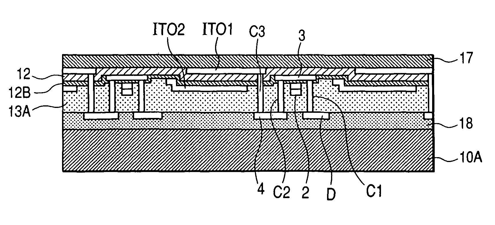
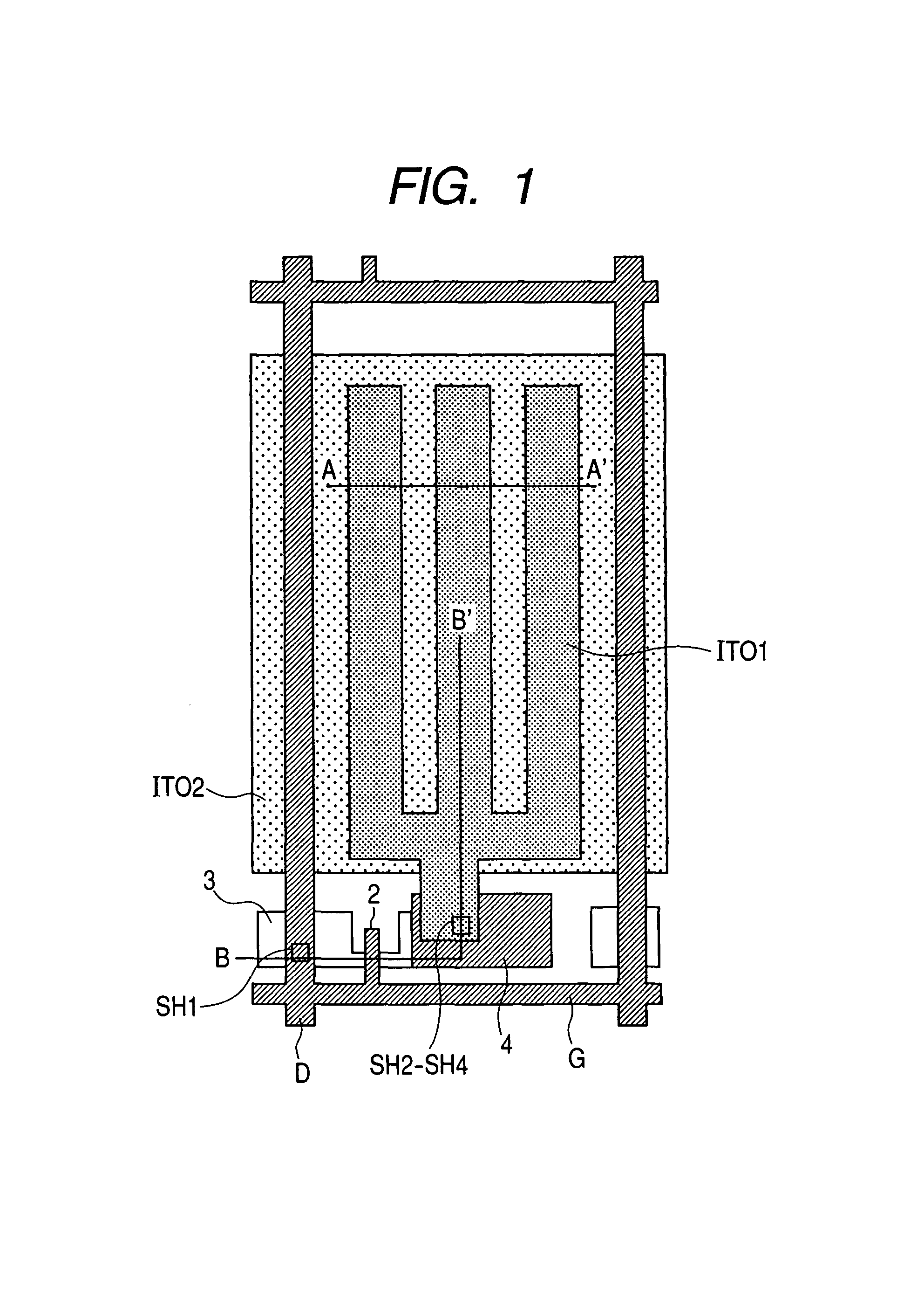
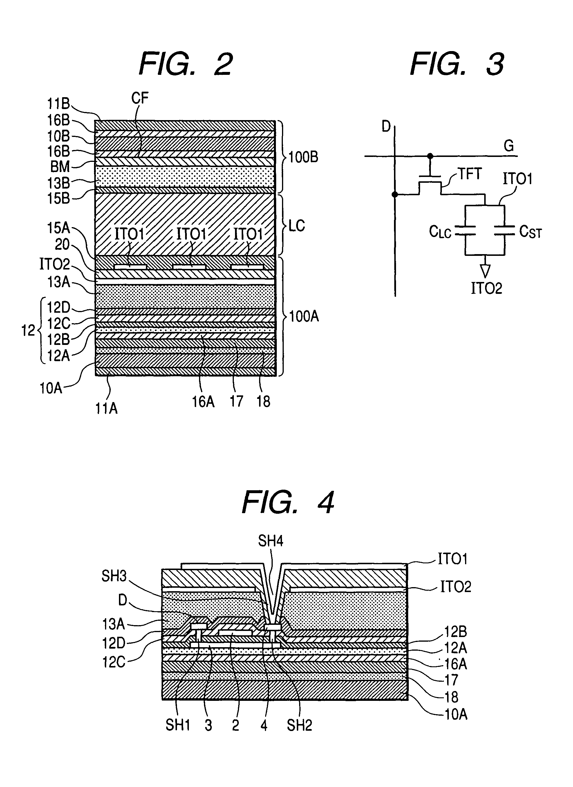
[0164]FIG. 1 is a plan view showing the constitution of 1 sub-pixel of a transmissive liquid crystal display panel according to an embodiment of the invention. FIG. 2 is a cross sectional view along line A-A′ shown in FIG. 1.

[0165]The structure of a liquid crystal display panel of this embodiment is to be described with reference to FIG. 2.

[0166]The liquid crystal display panel of this embodiment is an in-plane switching type liquid crystal display panel using a planar counter electrode, and the liquid crystal display panel has a transparent substrate (100B) and a transparent substrate (100A) arranged being opposed to each other by way of a liquid crystal layer LC. In this embodiment, the side of the main surface of the transparent substrate (100B) constitutes an observation side.

[0167]The transparent substrate 100B has a plastic substrate 10B and barrier layers 16B are formed to the upper and lower surfaces of the plastic substrate. On the side ...

third example

[0193]FIG. 6 shows a modified example for a method of forming a thin film transistor shown in FIG. 5 for the second embodiment. FIG. 6 shows a thin film transistor shown in FIG. 4 or FIG. 2 and a method of forming a liquid crystal device using the same.

[0194]In the same manner as the method shown in the second embodiment, a heat resistant transparent resin film 17 of the first embodiment was formed as a polymer film (a) above a glass substrate 19 as a support substrate. A barrier layer (inorganic layer) 16 was formed thereon in the same manner and a TFT portion was formed by a usual method in the same manner FIG. 5D. Then, an alignment layer 15A was formed and a rubbing treatment was applied.

[0195]SiON barrier layers of 100 nm thickness were formed on both surfaces of a plastic substrate 10B of 100 μm thickness and, using the same as a substrate, a black matrix BM layer and RGB color filter CF layer were formed by a usual method. The color filter portion 30 had an overcoat layer 13B...


PUM

PropertyMeasurementUnit
melting pointaaaaaaaaaa
temperatureaaaaaaaaaa
thicknessaaaaaaaaaa

Abstract

A method for manufacturing a thin film transistor including a step of forming a polymer film (a) to a layer above a support substrate, a step of forming a semiconductor element above the polymer film (a), and a step of separating the support substrate from the polymer film (a) formed with the semiconductor element in which the polymer film (a) has a thickness of 1 μm or more and 30 μm or less, a transmittance of 80% or higher to a visible light at a wavelength of 400 nm or more and 800 nm or less, a 3 wt % loss temperature of 300° C. or higher, and a melting point of 280° C. or higher.

Description

CLAIM OF PRIORITY[0001]The present application claims priority from Japanese patent application JP 2007-181829 filed on Jul. 11, 2007, the content of which is hereby incorporated by reference into this application.FIELD OF THE INVENTION[0002]The present invention concerns a method for manufacturing semiconductor devices including image display devices typically represented by liquid crystal devices. More specifically, the invention relates to a method of forming active matrix devices represented by thin film transistors (TFTs) on a flexible plastic substrate.BACKGROUND OF THE INVENTION[0003]For decreasing the weight of a flat panel display typically represented by a liquid crystal display device, it has been studied so far to decrease the thickness of a substrate, and liquid crystal display devices at present are manufactured by using a glass substrate having a thickness of about 0.5 mm to 1.1 mm. However, use of a glass substrate at the thickness less than that described above resu...

Claims


Application Information

Patent Timeline
Patent Type & Authority Patents(United States)
IPC IPC(8): G02F1/136H01L21/469H01L21/00G02F1/1333G02F1/1368G09F9/30H01L21/02H01L21/336H01L27/12H01L29/786
CPCH01L27/1214H01L27/1266G02F1/133305H01L29/78603H01L27/1218
Inventor HATTORI, TAKASHIHATANO, MUTSUKO
Owner PANASONIC LIQUID CRYSTAL DISPLAY CO LTD
Why Eureka
Try Eureka