Check patentability & draft patents in minutes with Patsnap Eureka AI!

Organic memory device and fabrication method thereof

a memory device and organic technology, applied in the field of organic memory devices, can solve the problems of increasing the production cost of memory chips, limited increasing the number of writing/erasing cycles, so as to achieve the effect of less complicated and/or less expensiv

Active Publication Date: 2012-07-10
SAMSUNG ELECTRONICS CO LTD
View PDF11 Cites 0 Cited by
  • Summary
  • Abstract
  • Description
  • Claims
  • Application Information

AI Technical Summary

Benefits of technology

[0013]Example embodiments are provided below for addressing certain of the deficiencies and/or limitations of the prior art memory devices through the manufacture and use of organic memory devices. Example embo...

Problems solved by technology

Conventional flash memories, however, have inherent technical limitations in that the number of writing / erasing cycles is limited, the writing speed is relatively slow, the production costs of memory chips may be increased as a result of the complicated processing currently required for attaining sufficiently high memory densities and certain physical limitations that impede further efforts toward miniaturization.
Other work has suggested an organic memory devices including organic active layers and a metal nanocluster applied between the organic active layers, but efforts in this area have been hampered by relatively low yields, difficulties in forming suitable metal nanoclusters, and reset voltages of about 0 V, rendering such devices generally unsuitable for widespread use as a nonvolatile organic memory.
Unlike metal filaments formed by a glow discharge polymerization technique, however, the formation of metal filaments within polystyrene films has not been demonstrated using more conventional coating techniques, e.g., spin coating or spin casting.
In each of these metal filament memories, however, the organic active layers of the conventional metal filament memory devices are formed using vacuum evaporation, and thereby requiring complicated fabrication processing and tending to increase fabrication costs relative to other conventional methods of forming organic layers, e.g., spin-coating.

Method used


Image

  • Organic memory device and fabrication method thereof
  • Organic memory device and fabrication method thereof
  • Organic memory device and fabrication method thereof

Examples


example 1

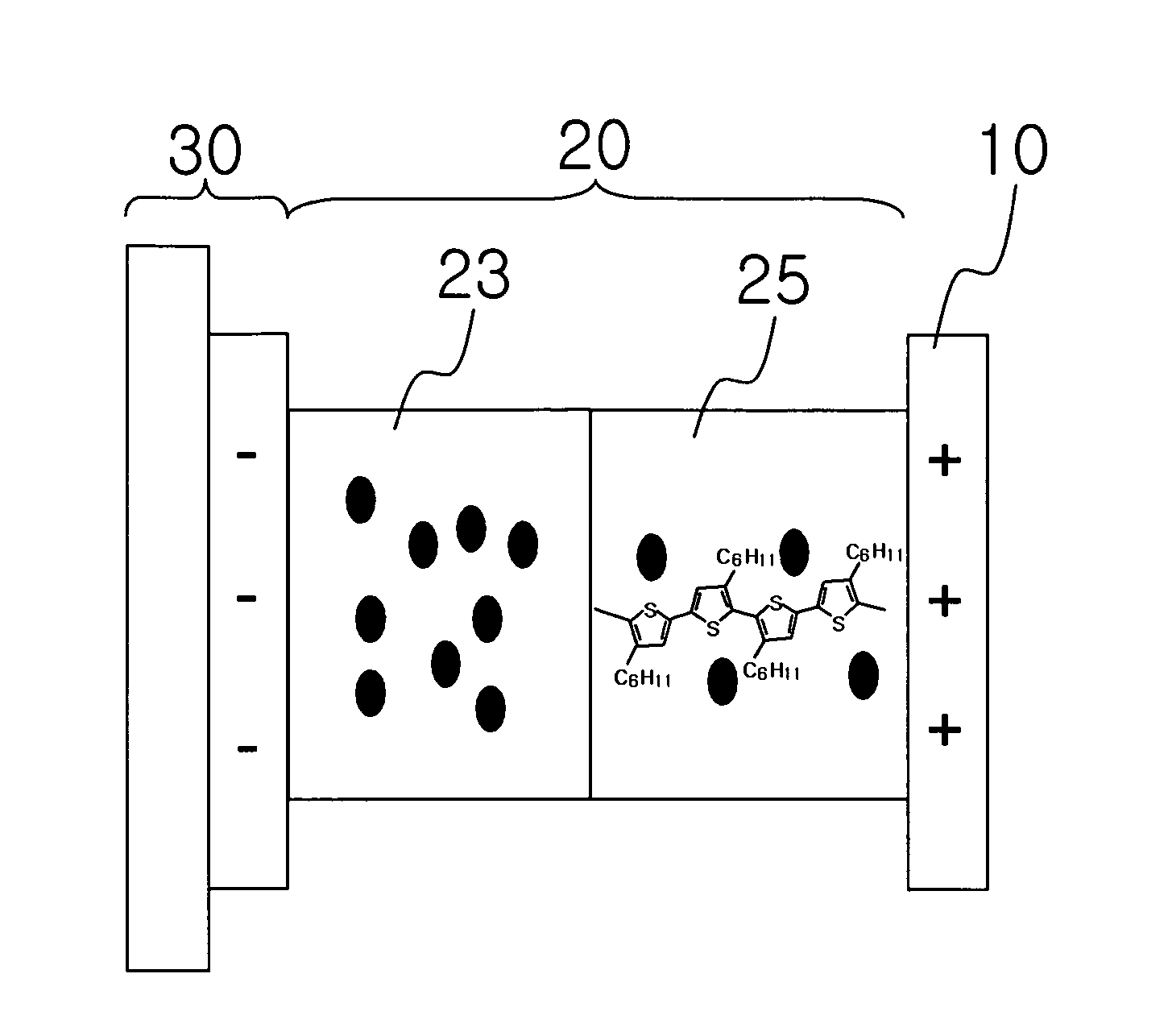
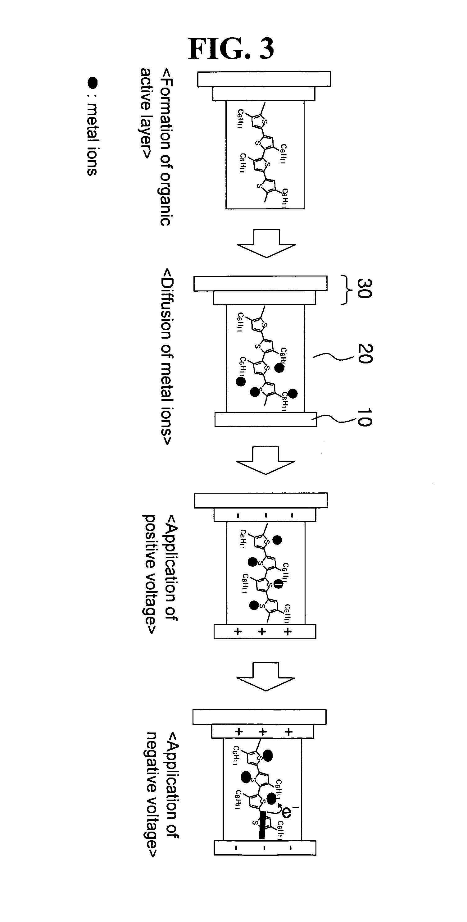
[0060]Aluminum was deposited to a thickness of about 80 nm on a glass substrate by thermal evaporation, patterned and etched to form a second electrode. An aqueous solution of polyaniline (2 wt %) was spin-coated at about 1,500 rpm on the patterned second electrode, and baked at about 130° C. for about 30 minutes to form a lower organic material layer. Subsequently, a chlorobenzene solution of poly-3-hexylthiophene (P3HT, about 0.5-1 wt %) was spin-coated at about 1,500 rpm on the lower organic material layer, and then baked at about 110° C. for about 30 minutes to form an upper organic material layer. Copper was then deposited on the organic active layer to a thickness of about 80 nm by thermal evaporation, patterned and etched to form a first electrode, thereby completing fabrication of an organic memory device of example embodiments. During fabrication of this organic memory device, the thicknesses of the lower and upper organic material layers were controlled to about 40 nm and ...

examples 2 and 3

[0061]Memory devices were fabricated in the same manner as described above in connection with Example 1, with the exception that the materials and thicknesses of the upper and lower organic material layers were changed to those indicated in Table 1.


PUM

PropertyMeasurementUnit
Electrical conductivityaaaaaaaaaa
Thicknessaaaaaaaaaa
Electrical conductivityaaaaaaaaaa

Abstract

Disclosed herein are an organic memory device and a method for fabricating the device. The organic memory device may include a first electrode, a second electrode and an organic active layer wherein the organic active layer includes an upper organic material layer formed of an electrically conductive organic material containing heteroatoms and a lower organic material layer formed of an electrically non-conductive organic material containing heteroatoms. Because the organic memory device exhibits improved thermal stability and non-volatility, it may be well suited for use in nonvolatile large-capacity storage units. Flexible electrodes may be used in the organic memory device to fabricate flexible memory devices.

Description

[0001]This non-provisional application claims priority under 35 U.S.C. §119 to Korean Patent Application No. 2006-10089, filed on Feb. 2, 2006, in the Korean Intellectual Property Office (KIPO), the entire contents of which are herein incorporated by reference.BACKGROUND[0002]1. Field[0003]Example embodiments relate to an organic memory device and a method for fabricating the device. Other example embodiments relate to an organic memory device including a first electrode, a second electrode and upper and lower organic material layers provided between the first and second electrodes wherein the upper organic material layer may be formed of an electrically conductive organic material containing heteroatoms and the lower organic material layer may be formed of an electrically non-conductive organic material containing heteroatoms, and a method for fabricating the organic memory device.[0004]2. Description of the Related Art[0005]With the recent dramatic developments in digital communic...

Claims


Application Information

Patent Timeline
IPC IPC(8): H01L51/30
CPCB82Y10/00G11C13/0014G11C13/0016H01L27/285G11C2213/56H01L51/0591H01L51/0035H01L51/0036G11C2213/77H10K19/202H10K85/111H10K85/113H10K10/50
Inventor JOO, WON JAELEE, SANG KYUN
Owner SAMSUNG ELECTRONICS CO LTD
Features
  • R&D
  • Intellectual Property
  • Life Sciences
  • Materials
  • Tech Scout
  • Unparalleled Data Quality
  • Higher Quality Content
  • 60% Fewer Hallucinations
Learn More