Power semiconductor devices

a technology of power semiconductors and semiconductor devices, applied in the direction of semiconductor devices, basic electric elements, electrical equipment, etc., can solve the problems of slow switching speed, current crowding, and complicated current gate control and di/dt/dt and dv/dt limitations, so as to improve paralleling turn, increase on-state resistance, and low spike current

Inactive Publication Date: 2012-07-17
CAMBRIDGE ENTERPRISE LTD
View PDF10 Cites 3 Cited by
  • Summary
  • Abstract
  • Description
  • Claims
  • Application Information

AI Technical Summary

Benefits of technology

[0012]Preferably each thyristor device has a gate width of between 50 μm and 1000 μm; preferably the gate width is greater than 150 μm. Preferably a MOS (metal oxide semiconductor) gate structure is employed which facilitates us of an IGBT (insulated gate bipolar transistor) fabrication process. A thyristor device may comprise multiple thyristor cells connected in parallel. Use of a wide gate structure facilitates a small latching current, clean turn-on, positive temperature coefficient, and high current and voltage slew rate capability. Broadly speaking, as the gate width increases so more P-i-N diode appears in series with the channel, facilitating achieving the desired temperature coefficient. A wide gate structure also facilitates rapid turn on and, in preferred embodiments, each thyristor device has a turn-on time of less than 10 μs. Some preferred embodiments have a turn-on time of less than 2 μs.
[0026]This may have a cell structure with dimensions comparable or larger than an IGBT cell. Cells are connected in parallel to form a chip with limited area for high yield. High current-rating modules are formed by paralleling several chips together. This structure facilitates adoption of an IGBT fabrication process.
[0027]The forth region may have a wide structure which contacts the second main electrode. The third region may also have a wide structure which is beneath the fourth region. This structure may be termed wide base structure. The wide structure of the third and the fourth regions may cause a sufficiently large so-called pinch resistance, that a voltage drop may be developed when a current flows to forward bias the third pn junction to latch up the device. When the third region is wide enough, the current required to latch up the device may be low enough. When the third region is narrow enough, the dv / dt limitation may be high enough. Therefore, a good trade off may be achieved, to concurrently have low latching current and high dv / dt rating.
[0029]P-i-N diode proportion to the whole device, (in contrast to the negative temperature coefficient in conventional thyristors, which causes current crowding in hotter devices). The wide gate structure may slightly increase on-state resistance, resulting in a very low spike current during latch up and improved paralleling turn on. The capacitance between the gate and the first electrode may be increased, which may reduce the Q factor of LCR series circuit during paralleling turn off. Hence the turn-off oscillation problem may be improved as well.
[0030]In embodiments an equivalent on-state voltage drop to conventional thyristors, a positive on-state resistance temperature coefficient, a small latching current and a small spike voltage during latch up may be provided. As previously mentioned, paralleled devices may be successfully turned on with small inductance of “IGBT” packaging. Current rating may be greatly increased by paralleling several chips in one module without too much increase in the cost and size of the system.

Problems solved by technology

However, thyristors have many drawbacks, such as slow switching speed, complicated current gate control and di / dt and dv / dt limitations.
It would be beneficial to be able to connect thyristors in parallel, but this results in current crowding, and generally the hottest device takes substantially all the current, resulting in thermal runaway.
Such devices do, however, have problems associated with them, as when the blocking voltage increases, the on-state voltage drop increases dramatically preventing their extending into the high voltage applications.
However, it has proved difficult in practice to produce a device which reliably meets the conflicting requirements mentioned above.
Those proposed devices either have a high on-state voltage drop due to the addition of a MOSFET in series with the thyristor structure, or have a complex fabrication process and drive circuitry due to dual gates or additional silicon layers.
Moreover it has proved difficult to adapt an IGBT process for the fabrication of thyristor devices.
The modern IGBT fabrication adopts the processes of an IC foundry and the area of an IGBT chip is limited within 2 cm2 due to the demand for high yield.
However, the paralleling of thyristors has many difficulties including both turn-on and turn-off failures, as well as uneven current sharing.
Because of these and other problems, no MOS-gated thyristor is yet commercially available.

Method used


Image

  • Power semiconductor devices
  • Power semiconductor devices
  • Power semiconductor devices

Examples


Embodiment Construction

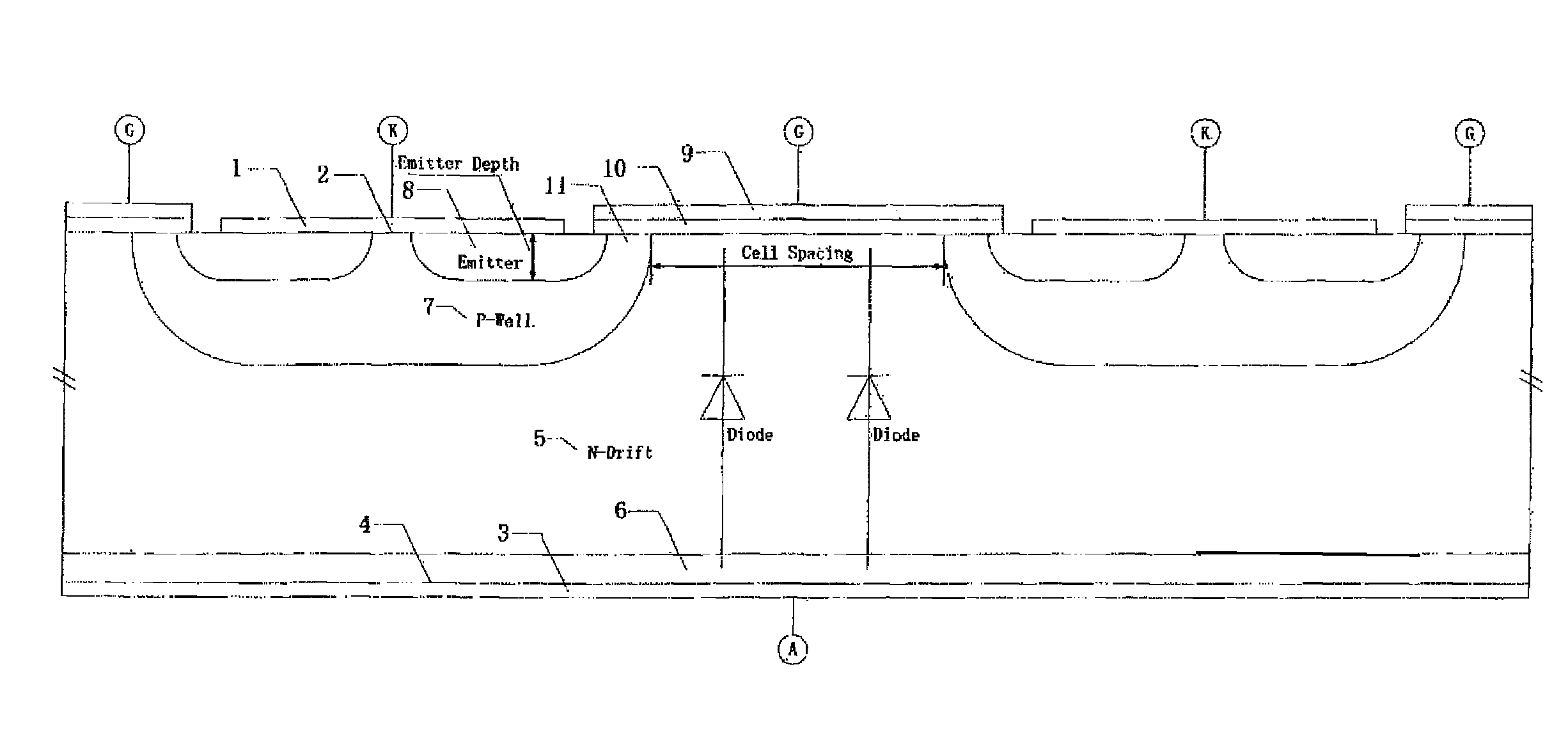
[0047]Broadly speaking we will describe a single gate MOS-gated thyristor with superior paralleling capability and an equivalent conduction property to conventional thyristors. With modified device structure and parameters, such as the wide gate and wide P base structure, superior characteristics are achieved. Due to the positive on-state resistance temperature coefficient and clean turn on characteristic, the devices can be fabricated using normal IGBT manufacturing process. Several chips can be connected in parallel in a module to enable high current handling capability while maintaining high manufacturing yield. The device demonstrates a potential to replace conventional thyristors for high power applications.

[0048]A half-cell structure of our MOS-gated thyristors has a basic PNPN thyristor structure and a MOS gate, which is similar to an IGBT. However, several important aspects have been changed and it possesses significant improvements. The pitch of the unit cell may range from...


PUM


Abstract

This invention generally relates to power semiconductor devices, and in particular to improved thyristor devices and circuits. The techniques we describe are particularly useful for so-called MOS-gated thyristors. We describe a thyristor comprising a plurality of power thyristor devices connected in parallel, each said thyristor device being operable at a device current which the device has an on-resistance with a positive temperature coefficient.

Description

RELATED APPLICATIONS[0001]This application is related to the following British patent application Serial No. GB0605632.9 filed Mar. 21, 2006 and U.S. Provisional patent application Ser. No. 60 / 784,201, filed Mar. 21, 2006; and which are incorporated herein by reference.FIELD OF THE INVENTION[0002]This invention generally relates to power semiconductor devices, and in particular to improved thyristor devices and circuits. The techniques we describe are particularly useful for so-called MOS-gated thyristors.BACKGROUND TO THE INVENTION[0003]Among existing power semiconductor devices, thyristors are one of the oldest types, which have superior on-state losses and the highest power-handling capability. However, thyristors have many drawbacks, such as slow switching speed, complicated current gate control and di / dt and dv / dt limitations. It would be beneficial to be able to connect thyristors in parallel, but this results in current crowding, and generally the hottest device takes substan...

Claims


Application Information

Patent Timeline
Patent Type & Authority Patents(United States)
IPC IPC(8): H01L29/74
CPCH01L29/7395
Inventor PALMER, PATRICK REGINALDWANG, ZHIHAN
Owner CAMBRIDGE ENTERPRISE LTD
Why Eureka
Try Eureka