SRAM device

a random access memory and sram technology, applied in semiconductor devices, digital storage, instruments, etc., can solve the problems of reducing the reliability of information systems, lowering the yield in the production process, and affecting the operation stability of sram, so as to increase the conductance of a selection transistor, and increase the read and write margins

Inactive Publication Date: 2012-08-14
NAT INST OF ADVANCED IND SCI & TECH
View PDF16 Cites 5 Cited by
  • Summary
  • Abstract
  • Description
  • Claims
  • Application Information

AI Technical Summary

Benefits of technology

[0019]According to this invention, the SRAM device which can increase both the read and write margins can be obtained. That is, according to the invention, unlike the SRAM device according to the related art, the conductance of a selection transistor can be increased in a SRAM cell during a writing operation, and decreased in the SRAM cell during a reading operation. As a result, it is possible to increase both the read and write margins at the same time. In addition, according to the invention as described in claim 4, it is possible to prevent an increase in current leakage in the selection transistors.

Problems solved by technology

The variation obviously affects the operation stability of the SRAM.
That is, the performances of the respective devices deviate randomly from the design target, so that mismatch occurs and bistability, which is indispensable for memory retention, is degraded.
The variation in the device characteristics may eventually lead to malfunction, so that the yield will be lowered in the production process and reliability of the information systems will be lowered.
The noise margin for a read operation, a read margin, is the most difficult to ensure sufficiently among read, write and hold operations.
The above-mentioned mismatch between the devices reduces the read margin.
This was because the transistor's characteristics are fixed and it was difficult to change the transistor's characteristics according to the read or write operations.
Still, there was a problem with the performance variation of the double gate field effect transistors, and no method has been provided which increases both the read margin and the write margin.
This circuit is too complicated as a circuit for increasing both the read and the write margins at the same time.

Method used


Image

  • SRAM device
  • SRAM device
  • SRAM device

Examples


first embodiment

(First Embodiment)

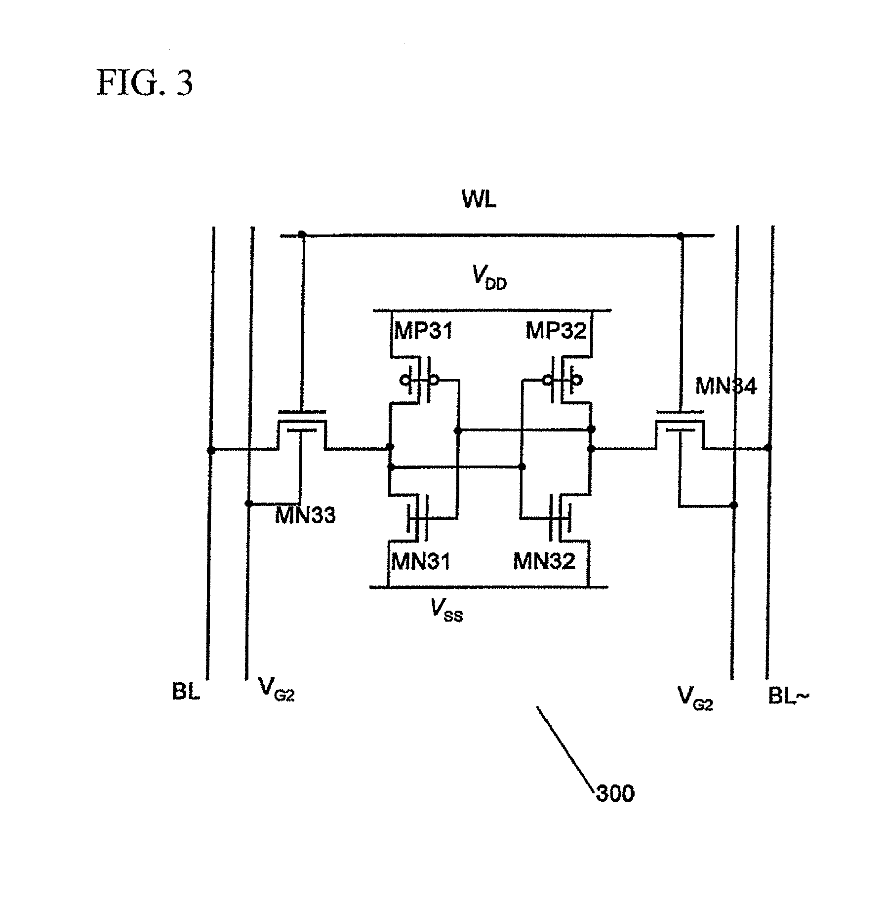
[0059]As described above, the four-terminal double gate field effect transistor is used as the selection transistor. Each transistor constituting flip-flops is configured with a usual double gate field effect transistor of which two gates are connected. As a result, a 6-transistor SRAM cell is configured as shown in FIG. 3.

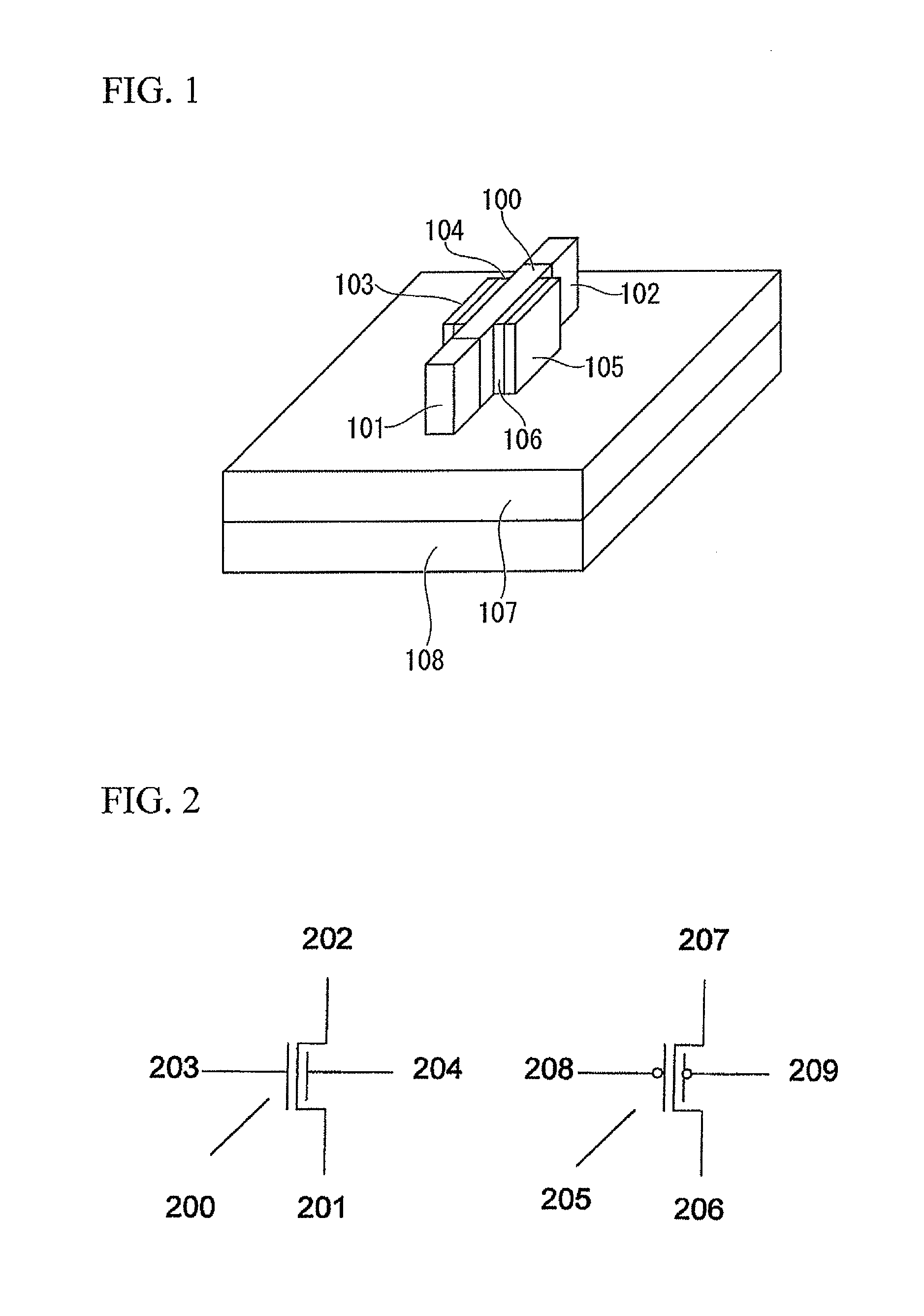
[0060]The terminals of the threshold voltage control gate of the four-terminal double gate field effect transistor, are connected to the wires parallel to bit lines BL and BL˜. Here, each MN31 and MN32 is different from the four-terminal double gate field effect transistor, and is a usual n-channel double gate field effect transistor of which two gates are connected to each other. MP31 and MP32 are the general p-channel double gate field effect transistors. In addition, the selection transistors MN33 and MN34 are the four-terminal double gate n-channel field effect transistors.

[0061]The SRAM cell shown in FIG. 3 is applied in the SRAM device show...

second embodiment

(Second Embodiment)

[0072]By selecting the capacitance of the gate insulating film and work function of the second gates 204 to 209 of the four-terminal double gate field effect transistor, the signal level, that is, the potential used in the VG2 and WL can be changed (refer to JP-A-2005-167163 and JP-A-2005-174960). Using this method appropriately, the invention can be applied even though either or both the VG2 and WL is changed in a range of VSS [=0]≦VG2≦VDD, VSS [=0]≦VWL≦VDD. Here, the configuration shown in FIG. 4 can be simplified as shown in FIG. 7. That is, the level shifter 401 is omitted from each row, and a CMOS inverter 701 shown in FIG. 8 is inserted instead of the level shifter 401 in each column, so that the same effect as that of the first embodiment can be attained. In FIG. 8, the MN71 is the n-channel field effect transistor, and the MP71 is the p-channel field effect transistor. Either the usual double gate field effect transistors or the conventional bulk planar MO...

third embodiment

(Third Embodiment)

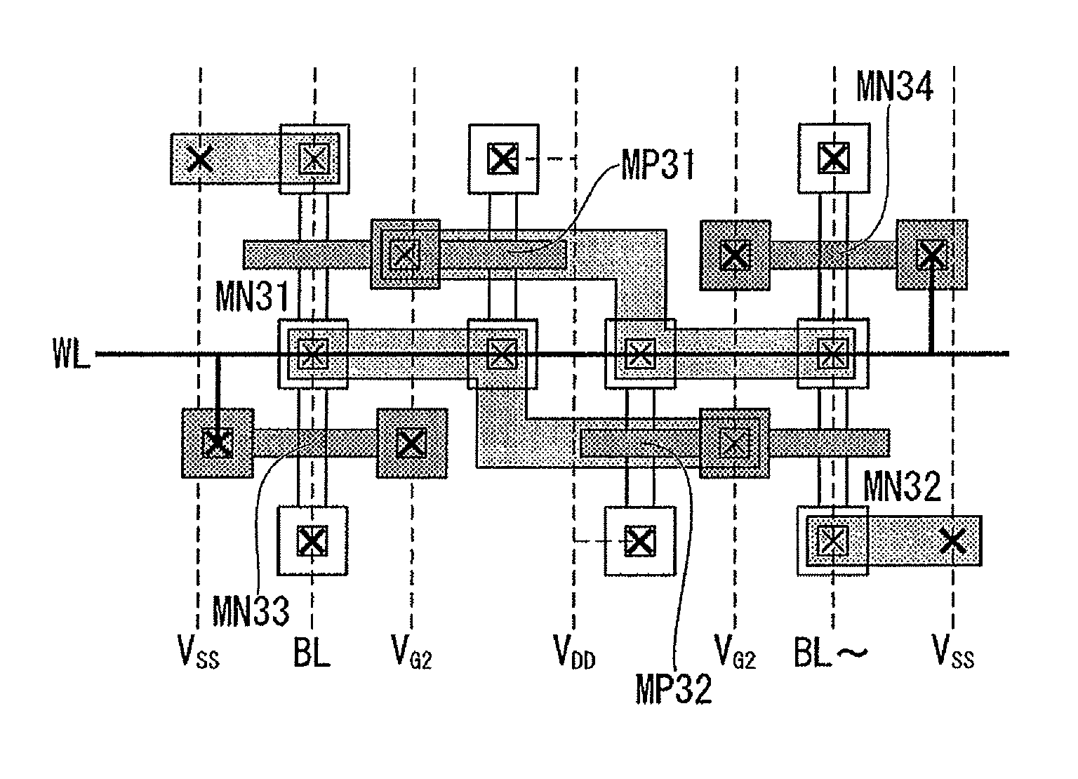
[0074]In this embodiment, a layout when a memory cell 300 is implemented on a semiconductor substrate in practice is disclosed. FIG. 10 is a figure illustrating the layout of the SRAM cell which is implemented on the semiconductor substrate. By configuring the four-terminal double gate field effect transistor so as to be symmetrical about a point, the memory cell shown in FIG. 3 is implemented on the semiconductor substrate. Further, in FIG. 10, wires in second and third metal layers are respectively denoted by a solid line and a dotted line so as to be simply displayed. In addition, the symbol x shown in FIG. 10 indicates the positions of contacts or via holes.


PUM


Abstract

An SRAM device uses a four-terminal double gate field effect transistor as a selection transistor, wherein the four-terminal double gate field effect transistor comprises a gate which drives the transistor and a gate which controls a threshold voltage, which are electrically separated from each other, on both surfaces of a standing semiconductor thin plate, and wherein a voltage used to reduce a threshold voltage is input to the gate which controls the threshold voltage of the selection transistor during a writing operation than during a reading operation. The SRAM device which can increase both the read and write margins is provided.

Description

CROSS REFERENCE TO RELATED APPLICATIONS[0001]The present application is a continuation under 37 C.F.R. §1.53(b) of prior application Ser. No. 12 / 531,780, filed Sep. 17, 2009, by Shinichi Ouchi et al. entitled SRAM DEVICE, which is a U.S.C. §371 National Phase conversion of PCT / JP2008 / 054720, filed Mar. 14, 2008, which claims priority of Japanese Application No. 2007-072903, filed Mar. 20, 2007, the entire contents of which are specifically incorporated by reference. The PCT International Application was published in the Japanese language.TECHNICAL FIELD[0002]The present invention relates to a static random access memory (SRAM) device.BACKGROUND ART[0003]Today, in conventional SRAM devices, 6-transistor CMOS SRAM cells are configured using planar MOS field effect transistors.[0004]However, miniaturization of the device dimensions, which is performed with the aim of performance improvement such as integration density and operation speed, increases variation in the characteristics of t...

Claims


Application Information

Patent Timeline
Patent Type & Authority Patents(United States)
IPC IPC(8): G11C11/00H01L27/088
CPCG11C11/412G11C11/413H01L27/11H01L27/1104H01L27/1203H01L29/785H10B10/00H10B10/12
Inventor OUCHI, SHINICHIMASAHARA, MEISHOKU
Owner NAT INST OF ADVANCED IND SCI & TECH
Why Eureka
Try Eureka