Method of manufacturing semiconductor device, and method of forming resist pattern

Inactive Publication Date: 2012-09-04
FUJITSU SEMICON LTD
View PDF13 Cites 0 Cited by
  • Summary
  • Abstract
  • Description
  • Claims
  • Application Information

AI Technical Summary

Benefits of technology

[0014]In the method of forming a resist pattern of the present invention, after a resist pattern smoothing material is applied to the surface of the resist pattern, heating and developing are carried out. At this time, at least one of the thickness of the application and the temperature of the heating is adjusted. When the resist pattern smoothing material is applied with a predetermined thickness on the surface of the resist

Problems solved by technology

In exposure techniques using the ArF Excier laser as the light source for selective exposure, however, a problem arises in that it is not possible to use resist materials which the light source for patterning has longer wavelength than the ArF Excimer laser.
Namely, such resist materials overly absorb the ArF Excimer laser and the light cannot be transmitted through these resist materials, such resist materials therefore do not function as resists when the ArF Excimer laser is utili

Method used


Image

  • Method of manufacturing semiconductor device, and method of forming resist pattern
  • Method of manufacturing semiconductor device, and method of forming resist pattern
  • Method of manufacturing semiconductor device, and method of forming resist pattern

Examples


example 1

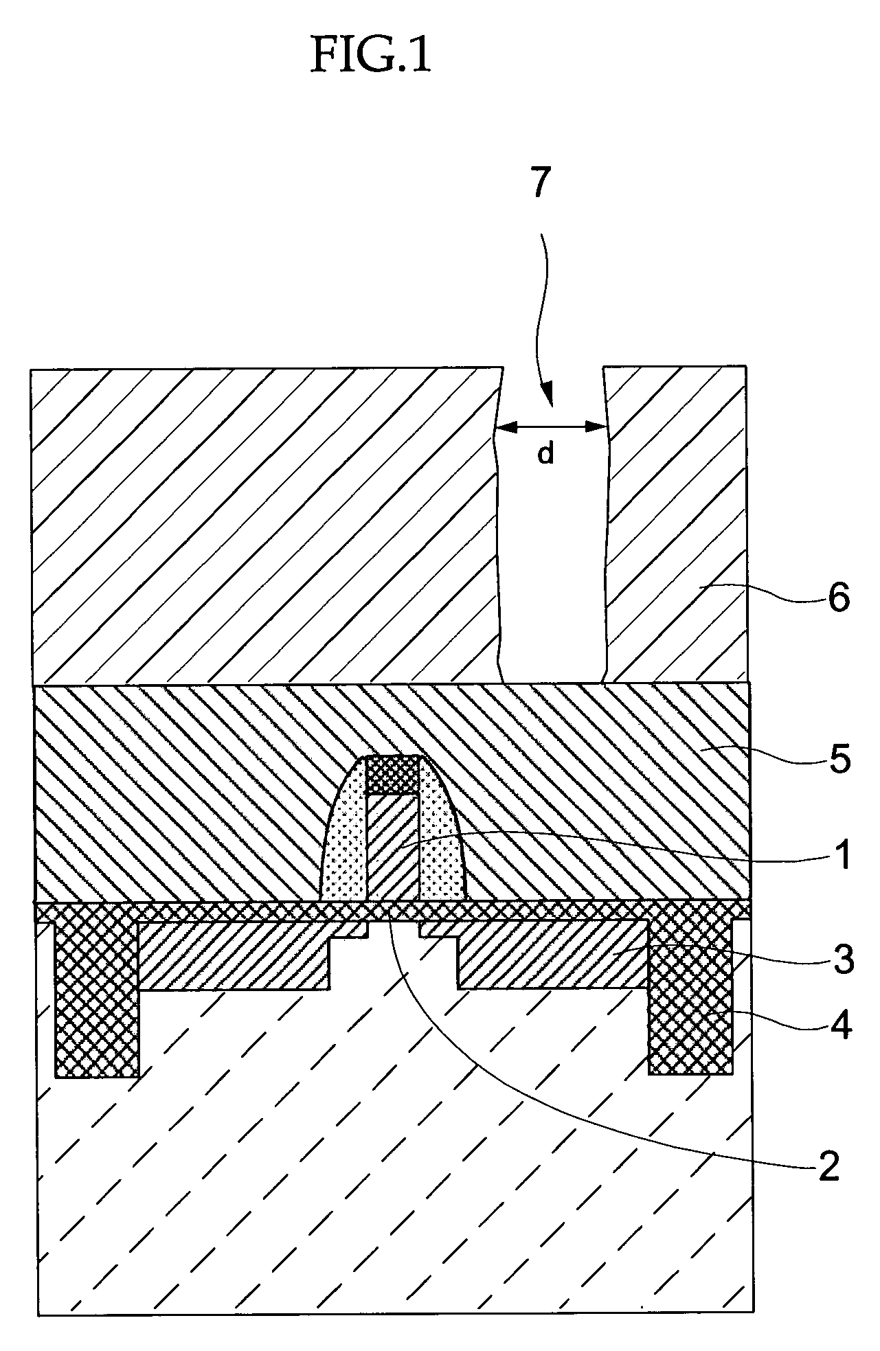
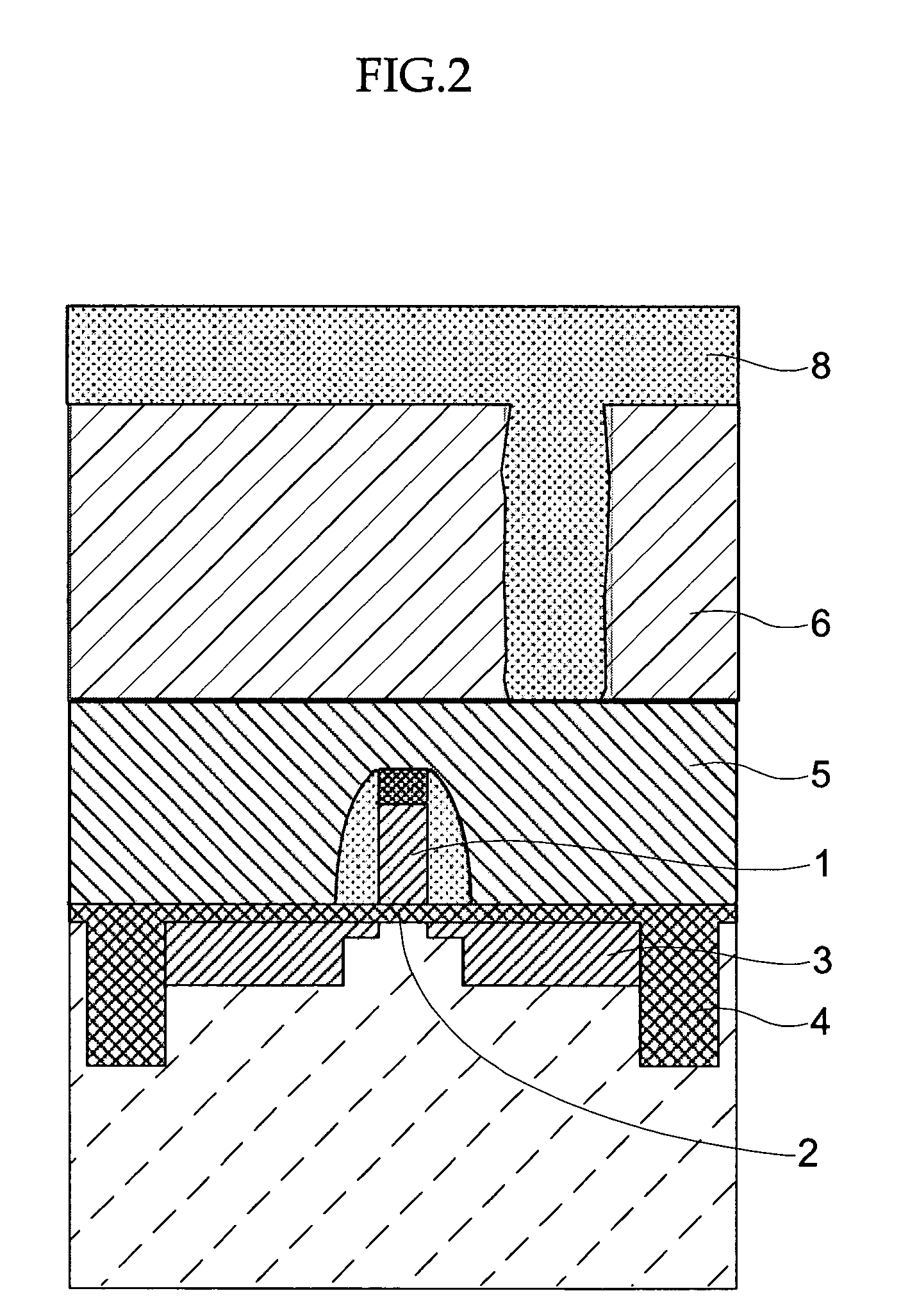
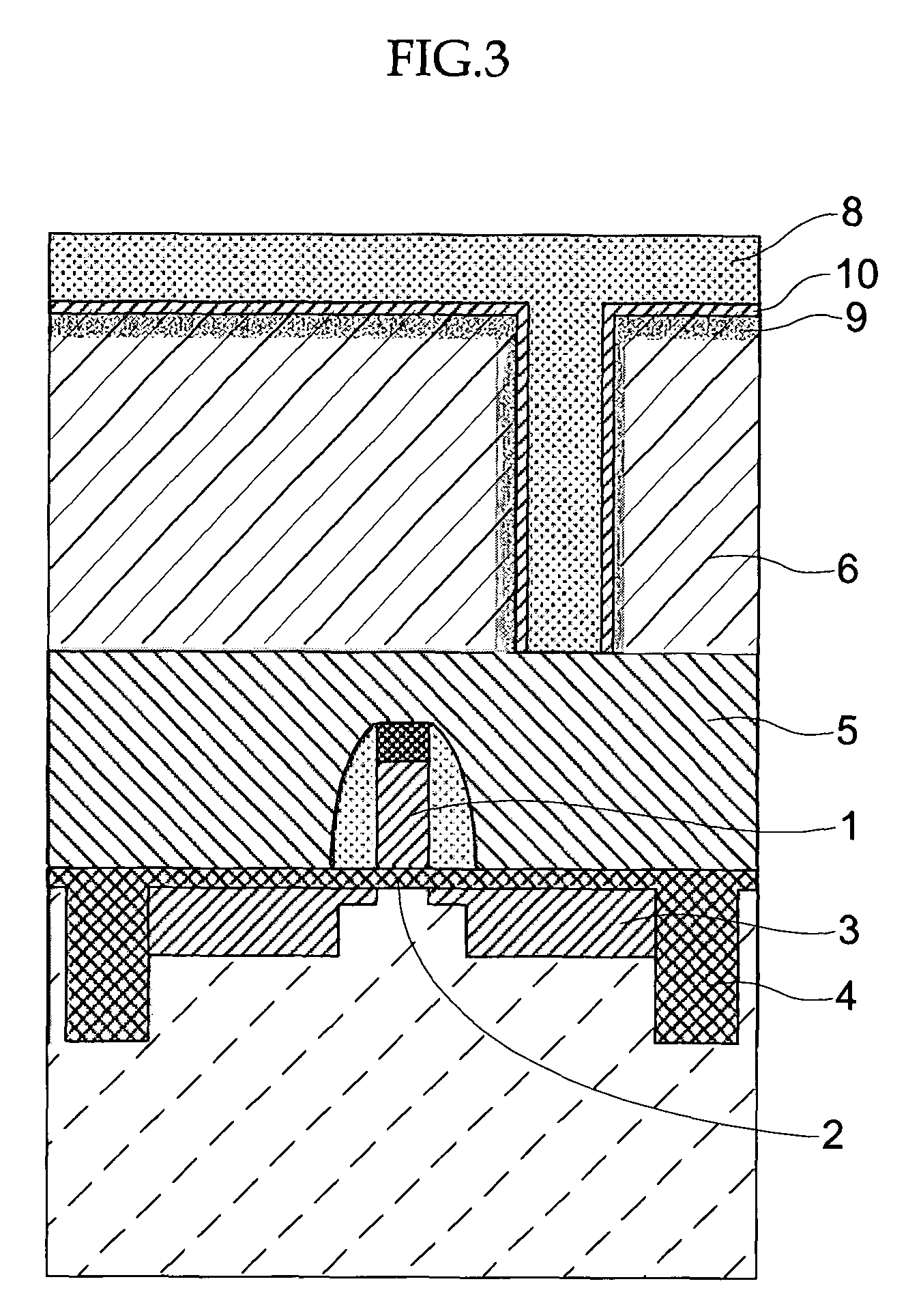
[0122]An ArF resist was applied onto a silicon wafer (a base layer). Selective exposure was carried out by using an ArF exposure device and developing was carried out, so as to form a resist pattern (hole pattern) (opening dimension=100 nm).

[0123]Next, a resist pattern smoothing material having the following composition was applied onto the surface of the resist pattern. Namely, the resist pattern smoothing material contained 16 parts by mass of polyvinyl acetal resin (KW-3, manufactured by Sekisui Chemical Co., Ltd.) as the resin, 1.16 parts by mass of tetramethoxymethyl glycol uril (manufactured by Sekisui Chemical Co., Ltd.) as the crosslinking agent, and 0.25 parts by mass of a polyoxyethylene monoalkylether surfactant (TN-80, a non-ionic surfactant manufactured by Asahi Denka Co., Ltd.) as the surfactant. Further, a mixed liquid of pure water (deionized water) and isopropyl alcohol (whose mass ratio was pure water (deionized water):isopropyl alcohol=98.6:0.4) was used as the ma...

example 2

[0133]A smoothed resist pattern was formed in the same way as in Example 1 except that the temperature for heating was made to be 90° C., the time for heating was made to be 60 seconds, and the application thickness of the resist pattern smoothing material was varied as shown in Table 2. The same evaluations as in Example 1 were carried out. The results are shown in Table 2.

[0134]

TABLE 2amount of variation inApplication thicknesssize (nm)edge roughness (nm)50 nm08.7 nm83 nm−23.7 nm98 nm−124.1 nm155 nm crosslinked over entire—surface

[0135]When the application thickness were 50 nm, 83 nm, 98 nm, 155 nm and the temperature for heating was 90° C. and the time for heating was 60 seconds, as compared with the cases in which the application thickness were 50 nm, 98 nm and 155 nm, in the case in which the application thickness was 83 nm, the amount of variation in the pattern size could be kept to within a range of ±10% (−2 nm) (i.e., Dav. (nm)≧D (nm)×(90 / 100) was satisfied), and the edge r...

example 3

[0136]A smoothed resist pattern was formed in the same way as in Example 1 except that the predetermined opening dimensions of the resist patterns were made to be 120 nm and 150 nm, the temperatures for heating were as shown in Table 3 (for opening dimension=120 nm) and Table 4 (for opening dimension=150 nm), the time for heating was 60 seconds, and the application thickness of the resist pattern smoothing material was 80 nm. The same evaluations as in Example 1 were carried out. The results are shown in Tables 3 and 4 and in FIG. 5.

[0137]

TABLE 3temperature foramount of variation inheating (baking)size (nm)edge roughness (nm) 80° C.−16.4 85° C.14.4 90° C.54.8 95° C.43.4100° C.173.9105° C.182.8110° C.253.1120° C.crosslinked over entirecrosslinked over entiresurfacesurface

[0138]

TABLE 4temperature foramount of variation inheating (baking)size (nm)edge roughness (nm)80° C.45.185° C.64.190° C.84.195° C.84.6100° C.203.2105° C.343.2110° C.373.3120° C.crosslinked over entirecrosslinked over...


PUM


Abstract

The present invention provides a method of manufacturing a semiconductor device capable of highly detailed patterning using a resist pattern having smoothed wall surfaces and reduced roughness. The method includes the steps of: forming a resist pattern over a base layer; applying a resist pattern smoothing material onto a surface of the resist pattern, thereafter heating and developing; and etching the base layer using the smoothed resist pattern, wherein one of an application thickness and a heat temperature is adjusted so as to smooth at least wall surfaces of the resist pattern. Aspects in which a maximum opening dimension and a minimum opening dimension of the smoothed resist pattern are ±5% of a predetermined opening dimension D (nm), and an average opening dimension Dav. (nm) of the smoothed resist pattern satisfies Dav. (nm)≧D (nm)×(90/100), are preferable.

Description

CROSS-REFERENCE TO RELATED APPLICATIONS[0001]This application is based upon and claims the benefits of the priority from the prior Japanese Patent Application No. 2002-248379, filed on Aug. 28, 2002, the entire contents of which are incorporated herein by reference.BACKGROUND OF THE INVENTION[0002]1. Field of the Invention[0003]The present invention relates to a method of forming a resist pattern which can easily and efficiently form a smoothed resist pattern in which a surface, at least wall surfaces, thereof is reduced its surface roughness and then smoothed. The present invention also relates to a method of manufacturing a semiconductor device which can efficiently manufacture a high-performance semiconductor device by carrying out a highly detailed patterning using a smoothed resist pattern formed by the aforementioned method of forming a resist pattern.[0004]2. Description of the Related Art[0005]In forming an extremely fine pattern on a semiconductor integrated circuit, a lith...

Claims


Application Information

Patent Timeline
IPC IPC(8): G03F7/26G03F7/40G03F7/16H01L21/027H01L21/311H01L21/312
CPCG03F7/168H01L21/0273H01L21/31144H01L21/312H01L21/02118
Inventor YAMAMOTO, HAJIMETAKECHI, SATOSHI
Owner FUJITSU SEMICON LTD
Why Eureka
Try Eureka