

Method for producing conductive coating film
a coating film and conductive technology, applied in the direction of conductive layers on insulating supports, non-metal conductors, conductors, etc., can solve the problems of inability to produce mass, inability to heat at high temperature, and inability to meet the requirements of mass production, etc., to achieve excellent adhesion, short time, excellent conductivity
- Summary
- Abstract
- Description
- Claims
- Application Information
AI Technical Summary
Benefits of technology
Problems solved by technology
Method used
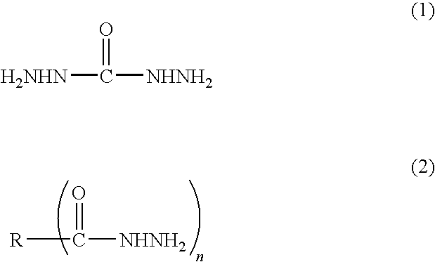
Image

Examples
example 1
[0162]60 parts of a cationic resin (Saftomer ST-3000, manufactured by Mitsubishi Chemical Co., Ltd; solid content 25%) as a material having anion exchange ability and 40 parts of a liquid medium (water / isopropyl alcohol=1 / 1, weight ratio) were mixed followed by stirring for 20 minutes with a dissolver to obtain a coating which contains a material having anion exchange ability. Next, this coating having anion exchange ability was applied on a polyester film (Ester E5100, manufactured by TOYOBO Co., Ltd.; 100 μm thickness) by a bar coater followed by drying for 5 minutes at 75° C. to obtain an anion exchange layer having coating film thickness of 6 μm after drying.
[0163]Thereafter, the dispersion of silver fine particles described in above Synthetic example 1 for preparing conductive fine particles was printed on the above anion exchange layer according to a dispenser method to form a circuit pattern of 3 mm in width, followed by drying it for 10 minutes in a hot air oven at 120° C. t...
example 2
[0164]7.5 parts of polyvinyl alcohol resin (Poval PVA-117, manufactured by Kuraray Co., Ltd.) as the other resin, 2.5 parts of a quaternary ammonium salt (Quartamin 24P, manufactured by Kao Corporation) as a material having anion exchange ability and 90 parts of a liquid medium (water / isopropyl alcohol=1 / 1) were mixed followed by stirring it for 60 minutes by a dissolver to obtain a coating which contains a material having anion exchange ability. Next, this coating having anion exchange ability was applied on a glass plate according to a spin coating method followed by drying it for 5 minutes at 75° C. to obtain an anion exchange layer having a coating film thickness of 6 μm after drying.
[0165]Thereafter, the dispersion of silver fine particles described in above Synthetic example 2 for preparing conductive fine particles was applied on the above anion exchange layer according to a spin coating method, followed by drying it for 10 minutes in a hot air oven at 150° C. to obtain a con...
example 3
[0166]15 parts of a cationic resin (Pulset JK-510, manufactured by Meisei Chemical Works, Ltd.; solid content 20%) as a material having anion exchange ability, 60 parts of colloidal silica (Snowtex O, manufactured by Nissan Chemical Industries, Ltd.; solid content 20%) as a material having no anion exchange ability, and 25 parts of a liquid medium (water / isopropyl alcohol=1 / 1) were mixed followed by stirring it for 20 minutes by a dissolver to obtain printing ink which contains a material having anion exchange ability. Next, this printing ink having anion exchange ability was solid printed on an entire surface of a polyester film (Ester E5100, manufactured by TOYOBO Co., Ltd.; 100 μm thickness) by a small gravure printer, followed by drying it to obtain an anion exchange layer having a coating film thickness of 5 μm. The drying temperature of the printer was set at 60° C.
[0167]Thereafter, the gravure printing was conducted on the above anion exchange layer by a small gravure printer...
PUM
| Property | Measurement | Unit |
|---|---|---|
| particle diameter | aaaaa | aaaaa |
| thickness | aaaaa | aaaaa |
| temperature | aaaaa | aaaaa |
Abstract
Description
Claims
Application Information