
Photoelectric conversion film, photoelectric conversion device and color image sensor having the photoelectric conversion device

a conversion device and photoelectric technology, applied in thermoelectric devices, radiation controlled devices, nanoinformatics, etc., can solve the problems of low sensitivity reduced performance of light receiving devices, false color phenomena, etc., to increase the number of pixels, improve definition, and increase the external quantum efficiency

Active Publication Date: 2012-11-27
SAMSUNG ELECTRONICS CO LTD +1
View PDF6 Cites 0 Cited by
  • Summary
  • Abstract
  • Description
  • Claims
  • Application Information

AI Technical Summary

Benefits of technology

The patent describes a photoelectric conversion film and a device that includes it. The film is made up of layers that can absorb different colors of light and convert them into electrical signals. The device includes electrodes and a buffer layer, hole transfer layer, or electron transfer layer to improve the performance of the device. The technical effect of this patent is to provide a photoelectric conversion film that can selectively absorb blue and green light and has high external quantum efficiency, resulting in improved image quality and increased efficiency in using light.

Problems solved by technology

In these structures, a pixel size can be reduced and thus a light quantity reaching the Si-optical diode decreased, thereby causing a decrease in the performance of the light receiving device.
As a result, the light receiving device can have low sensitivity, exhibit a false color phenomenon, a moiré phenomenon and low resolution.

Method used


Image

  • Photoelectric conversion film, photoelectric conversion device and color image sensor having the photoelectric conversion device
  • Photoelectric conversion film, photoelectric conversion device and color image sensor having the photoelectric conversion device
  • Photoelectric conversion film, photoelectric conversion device and color image sensor having the photoelectric conversion device

Examples


example 1

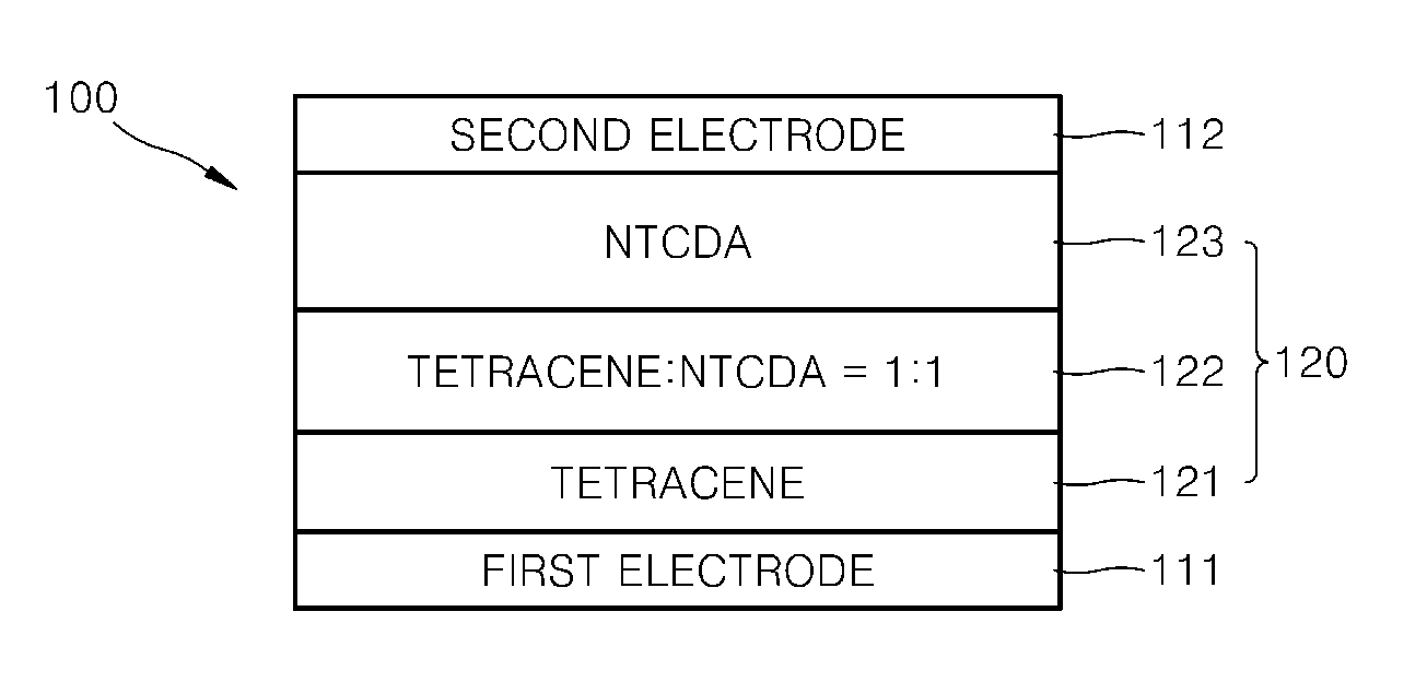
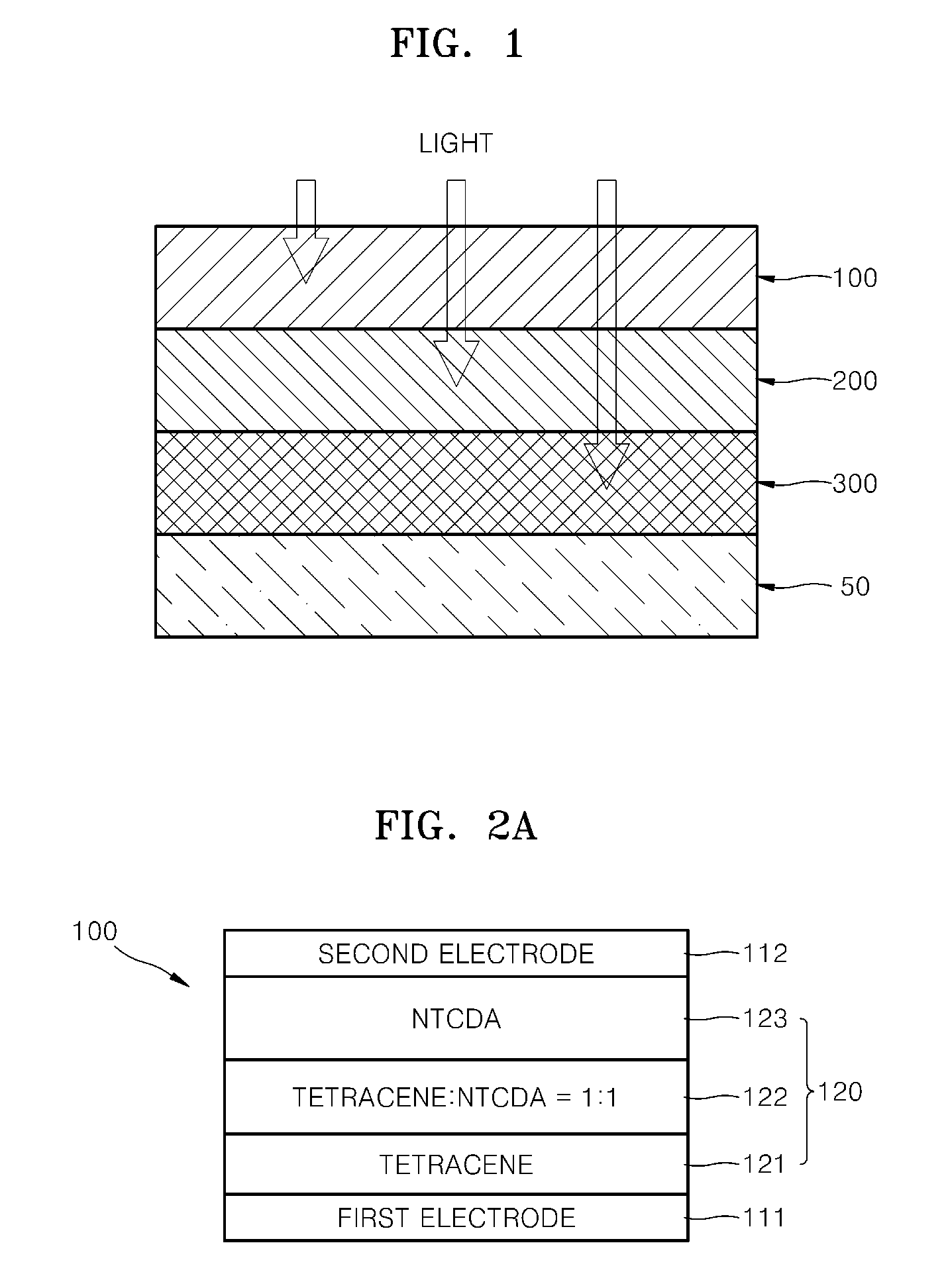
Manufacture of the First Blue Color Photoelectric Conversion Device 100 Illustrated in FIG. 2A

[0058]Tetracene is deposited on a glass substrate, on which an ITO electrode (the first electrode 111) is disposed, to a thickness of 30 nm, to form the p-type layer 121. Then, tetracene and NTCDA are co-deposited on the p-type layer 121 to a thickness of 100 nm to form the p,n-type layer 122. Then, NTCDA is deposited on the p,n-type layer 122 to a thickness of 250 nm to form the n-type layer 123. Then, an Ag electrode (the second electrode 112) is disposed on the n-type layer 123 with a thickness of 20 nm. The glass substrate, on which the ITO electrode is disposed, is cleaned using water, ultrasonic waves, methanol and acetone. The cleaned glass substrate is then O2 plasma processed. Then, a thermal evaporator is used to sequentially deposit organic materials on the ITO electrode disposed on the O2 plasma processed glass substrate under a pressure of 1×10⁻⁵ torr at a deposition speed of 2...

example 2

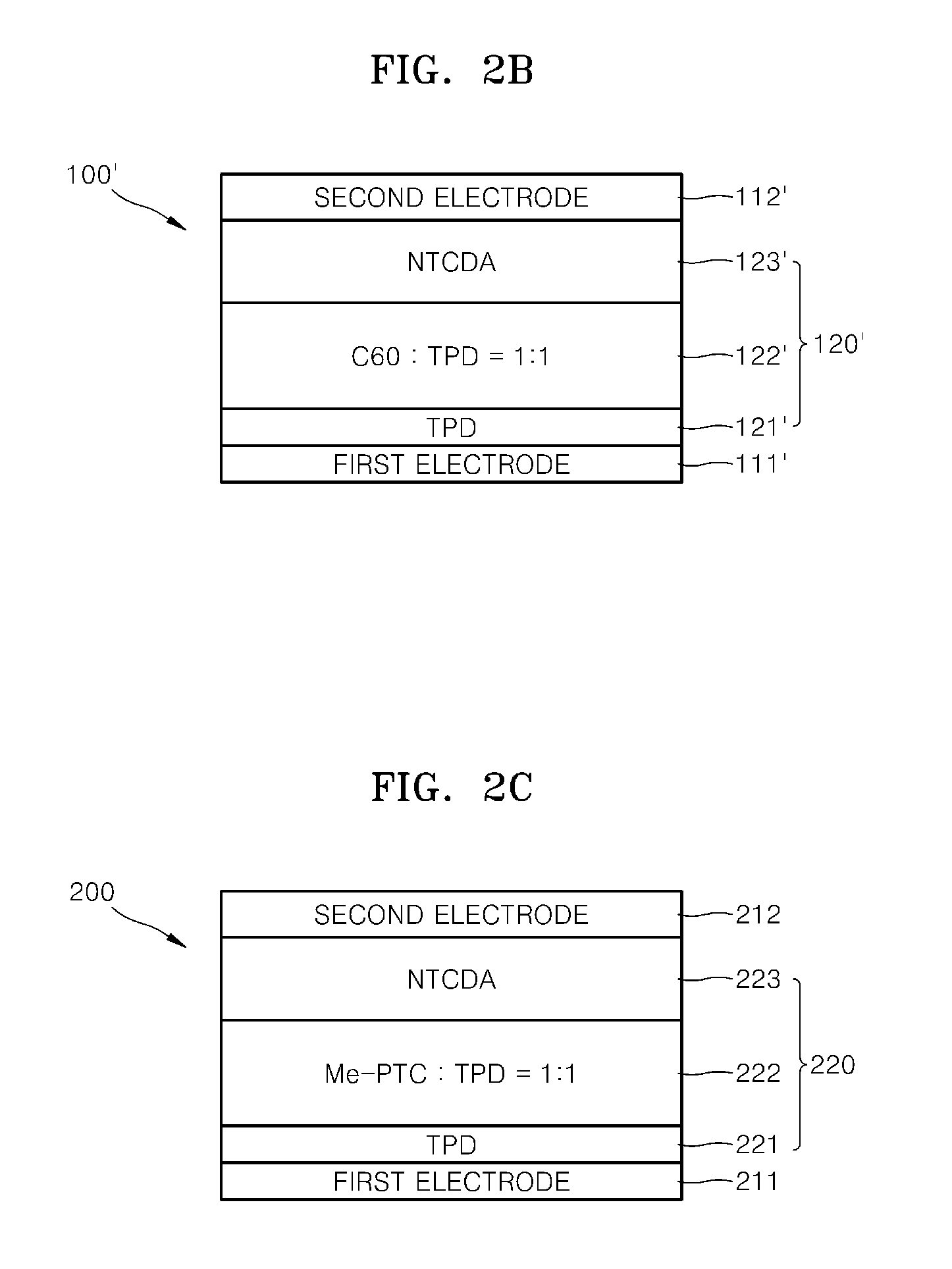
Manufacture of the Second Blue Color Photoelectric Conversion Device 100′ Illustrated in FIG. 2B

[0059]The second blue color photoelectric conversion device 100′ is manufactured in the same manner as in Example 1, except that TPD is deposited to form the p-type layer 121′, TPD and C60 are co-deposited to form the p,n-type layer 122′ and NTCDA is deposited to form the n-type layer 123′.

example 3

Manufacture of the Green Color Photoelectric Conversion Device 200 Illustrated in FIG. 2C

[0060]The green color photoelectric conversion device 200 is manufactured in the same manner as in Example 1, except that TPD is deposited to form the p-type layer 221, TPD and Me-PTC are co-deposited to form the p,n-type layer 222 and NTCDA is deposited to form the n-type layer 223.

[0061]Electrical Characteristics Measurement

[0062]An electrometer (Keithley model 485) is used to measure electrical characteristics of the photoelectric conversion devices manufactured as in Examples 1 through 3 under a pressure of 1×10⁻⁵ torr and the results are shown in FIGS. 3A through 3C. A xenon lamp and a monochrometer are used to provide monochromatic light and a function generator (Hokudo Denko, Ltd., HB-104) is used. FIGS. 3A through 3C are graphs showing external quantum yields (“External QE”) of the photoelectric conversion devices manufactured as in Examples 1 through 3. More specifically, FIG. 3A is a g...


PUM


Abstract

A blue color photoelectric conversion film includes: a p-type layer formed by depositing tetracene; a p,n-type layer formed by co-depositing tetracene and naphthalene-tetracarboxylic-dianhydride (“NTCDA”) on the p-type layer; and an n-type layer formed by depositing NTCDA on the p,n-type layer.

Description

CROSS-REFERENCE TO RELATED APPLICATION[0001]This application claims priority to Korean Patent Application No. 10-2008-0108509, filed on Nov. 3, 2008, and all the benefits accruing therefrom under 35 U.S.C. §119, the contents of which in their entirety are herein incorporated by reference.BACKGROUND[0002]1. Field[0003]This disclosure relates to a photoelectric conversion film, a photoelectric conversion device including the photoelectric conversion film, and a color image sensor including the photoelectric conversion device.[0004]2. Description of the Related Art[0005]Light receiving devices are used in digital cameras, broadcasting cameras, surveillance cameras, computer web cameras, camcorders, automotive sensors, household sensors and solar batteries. Generally, such light receiving devices include a micro lens, a color filter and a Si-optical diode. In these structures, a pixel size can be reduced and thus a light quantity reaching the Si-optical diode decreased, thereby causing ...

Claims


Application Information

Patent Timeline
Patent Type & Authority Patents(United States)
IPC IPC(8): H01L51/00H10K99/00
CPCH01L51/0059Y02E10/50B82Y10/00H01L51/0054Y02E10/549H01L51/4253H01L51/424H01L51/0046H10K85/211H10K85/622H10K85/631H10K30/20H10K30/30H10K39/32H01L27/146
Inventor KIM, KYU-SIKHIRAMOTO, MASAHIRO
Owner SAMSUNG ELECTRONICS CO LTD
Learn More