

Polymeric coating of substrate processing system components for contamination control
a technology of substrate processing system and contamination control, applied in the direction of superimposed coating process, instruments, transportation and packaging, etc., can solve the problems of affecting the performance of devices formed on the substrate surface, so as to reduce the chance of transferring carbon, and reduce the porosity
- Summary
- Abstract
- Description
- Claims
- Application Information
AI Technical Summary
Benefits of technology
Problems solved by technology
Method used
Image

Examples
Embodiment Construction
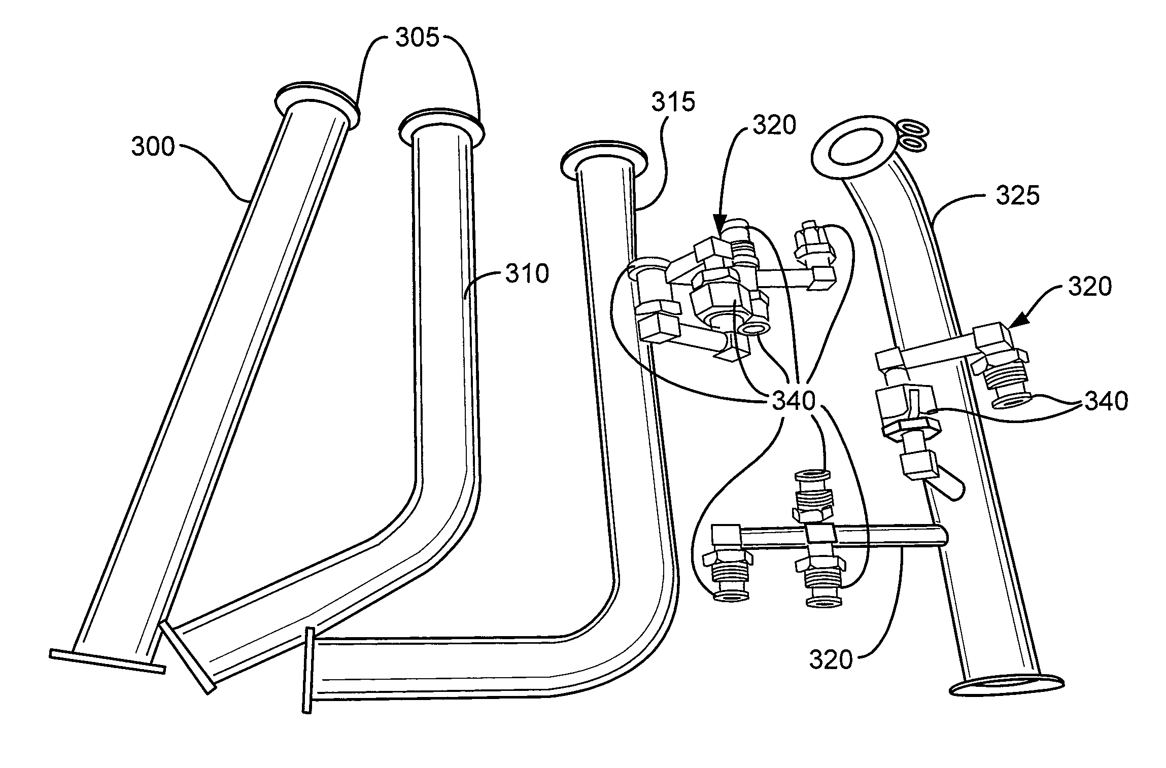
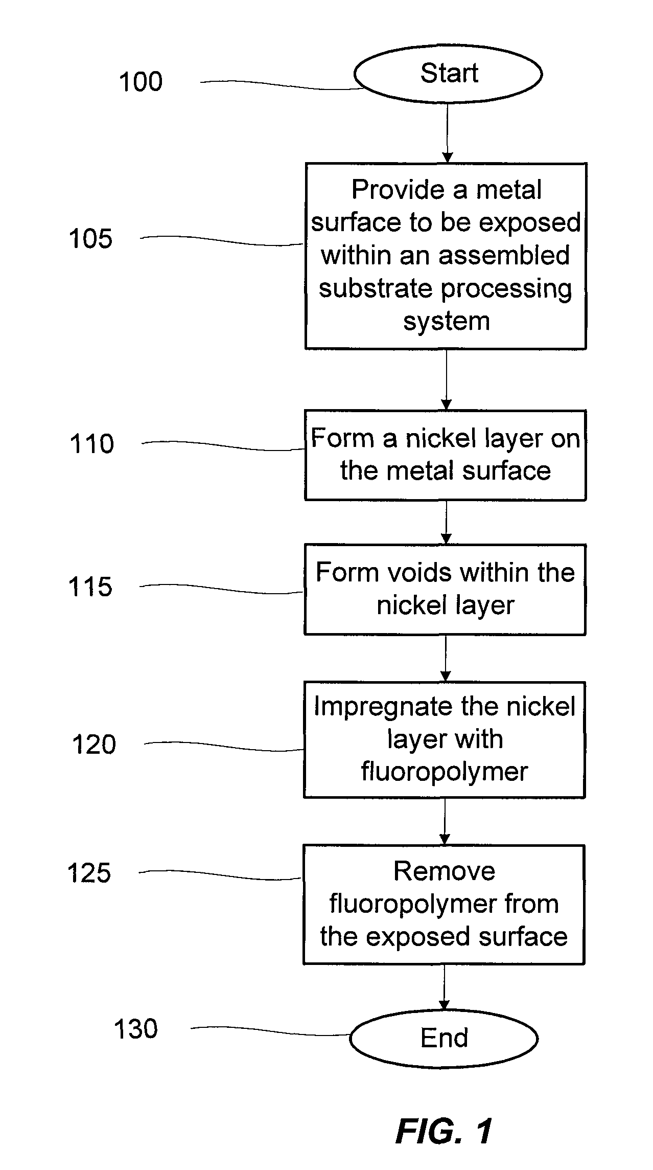
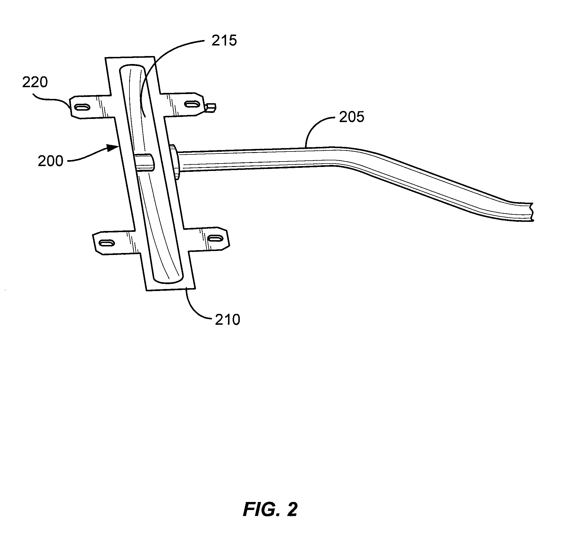
[0022]Aspects of the disclosure pertain to thin protective coatings (and their methods of deposition) for metal components used in substrate processing. The coatings may comprise nickel (Ni) and fluoropolymer and may be thinner than dimensional tolerances of the metal components. The coatings may also adhere to the underlying metal surfaces more strongly than common polymeric coatings. The coatings may possess a reduced exposed polymer to reduce the chance of transferring carbon to the substrate surface. Other advantages of the coatings are a reduced porosity, which reduces the potential for gases to penetrate through the film and compromising the physical integrity of the coating-metal interface. Coatings may exhibit a very smooth surface to slow the accumulation of deposits on the interior walls of chamber components and may be hydrophobic to limit or slow the absorption of water during cleaning procedures. Additional benefits include a high lubricity, which is helpful in regions ...
PUM
| Property | Measurement | Unit |
|---|---|---|
| thick | aaaaa | aaaaa |
| thick | aaaaa | aaaaa |
| thick | aaaaa | aaaaa |
Abstract
Description
Claims
Application Information