Layered chip for use in soldering

a layer chip and metal chip technology, applied in the field of layer metal chips, can solve the problems of weakening affecting the electrical conductivity of the soldering connection, and affecting the mechanical strength and/or electrical conductivity of the soldering connection, and achieves the effects of simple and cost-effective production, good electrical conductivity, and reliable soldering

Active Publication Date: 2013-01-15
SEMIKRON ELECTRONICS GMBH & CO KG
View PDF10 Cites 4 Cited by
  • Summary
  • Abstract
  • Description
  • Claims
  • Application Information

AI Technical Summary

Benefits of technology

[0007]It is an object of the invention to eliminate the disadvantages according to the prior art. In particular, the intention is to produce a chip which can be produced as simply and cost-effectively as possible and which can be reliably soldered. In particular, in the case of a multiple soldering, the intention is to ensure a soldering connection having a strong mechanical connection and good electrical conductivity.
[0008]In accordance with the invention, it is provided that the soldering layer has at least one interface formed by interrupting the performance of the coating method. It has surprisingly been found that such a soldering layer formed from a plurality of layers separated in each case by an internal interface makes it possible to prevent an undesired penetration of a melt formed from the soldering layer and a solder through subsequent metal layers applied on the substrate body. The inventive chip can be produced simply and cost-effectively. All that is necessary for this purpose is to interrupt the performance of the coating method during the production of the soldering layer, such that at least one internal interface is formed within a single soldering layer. A barrier forms within the soldering layer in the region of the internal interface, which barrier blocks an advance of a melt formed from the solder and the partly melted soldering layer in the direction of the chip body. As a consequence of this, contact of the melt with subsequent metal layers provided on the chip body does not occur or occurs only to a very small extent. An undesired formation of voids and / or pores within the layer assemblage, as caused by such contact, can thus be dependably and reliably avoided. The chip proposed is distinguished by a high process reliability, particularly in such production processes in which the chip is repeatedly exposed to temperatures in the range of from about 200 to about 250° C.
[0011]According to a further configuration of the invention, a second intermediate layer can be provided between the noble metal layer and the soldering layer, the second intermediate layer being formed substantially from titanium. The further intermediate layer contributes to further improvement of the process reliability.
[0016]Advantageously, a thickness of the soldering layer is from about 0.7 to about 1.2 μm, preferably from about 0.8 to about 1.0 μm. The soldering layer is thus embodied with approximately just the same thickness as a soldering layer which has been used hitherto according to the prior art and which is produced in an uninterrupted coating operation. Despite the approximately same layer thickness as in the case of the soldering layer according to the prior art, the soldering layer according to the invention has a considerably improved resistance to penetration of a melt formed from the soldering layer and the solder.

Problems solved by technology

In this case, it may happen that the layer assemblage produced from the metallic layers, in particular, is heated repeatedly to a temperature of from about 200 to about 250° C. When a soldering connection that has already been produced is reheated, it can happen that a new melt forms from the soldering layer and the solder advances in the direction of the chip body and penetrates through further metallic layers of the layer assemblage in an undesirable manner.
Consequently, voids or pores can form within the layer assemblage.
Such voids or pores weaken the mechanical strength and / or electrical conductivity of the soldering connection.

Method used


Image

  • Layered chip for use in soldering
  • Layered chip for use in soldering

Examples


Embodiment Construction

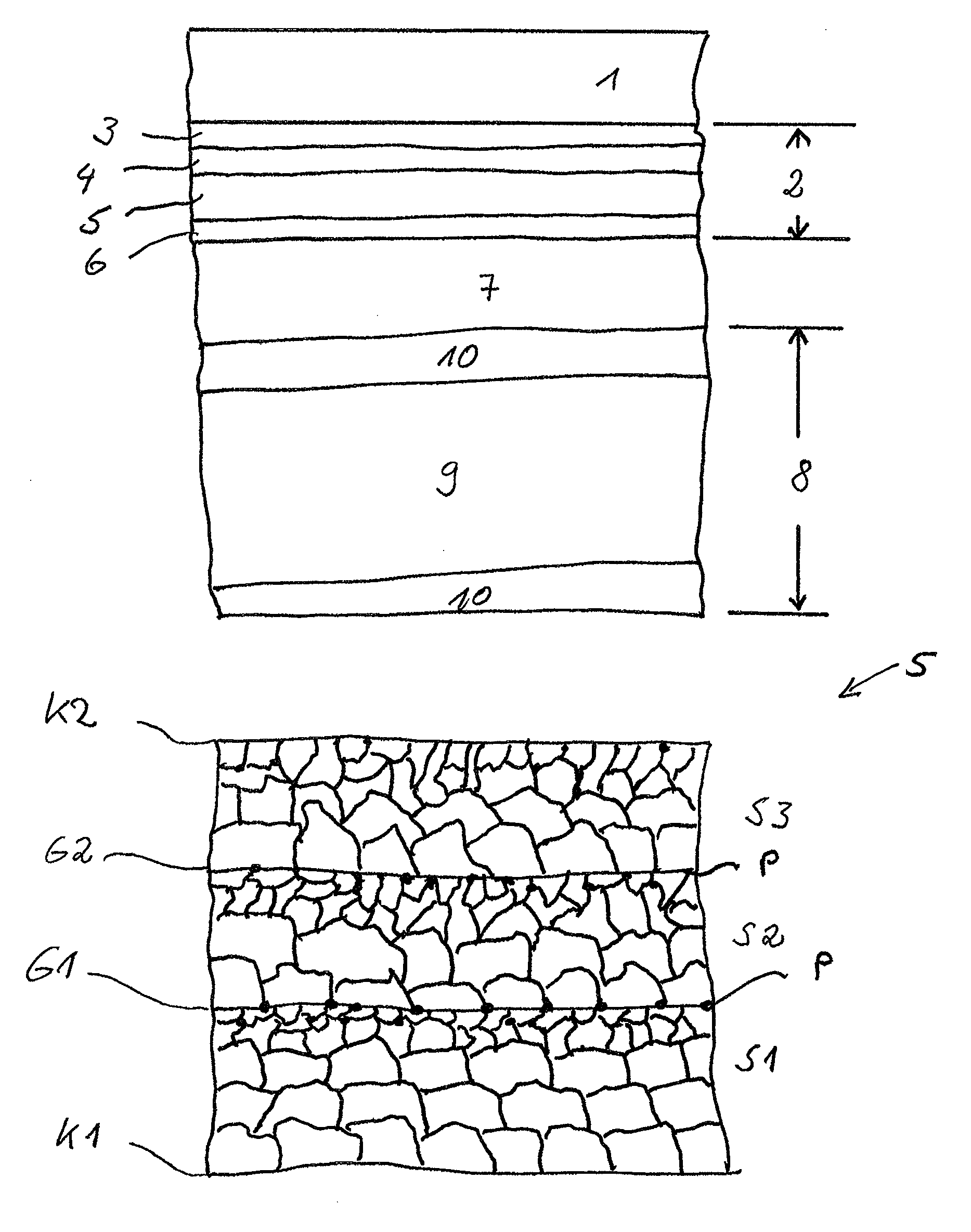
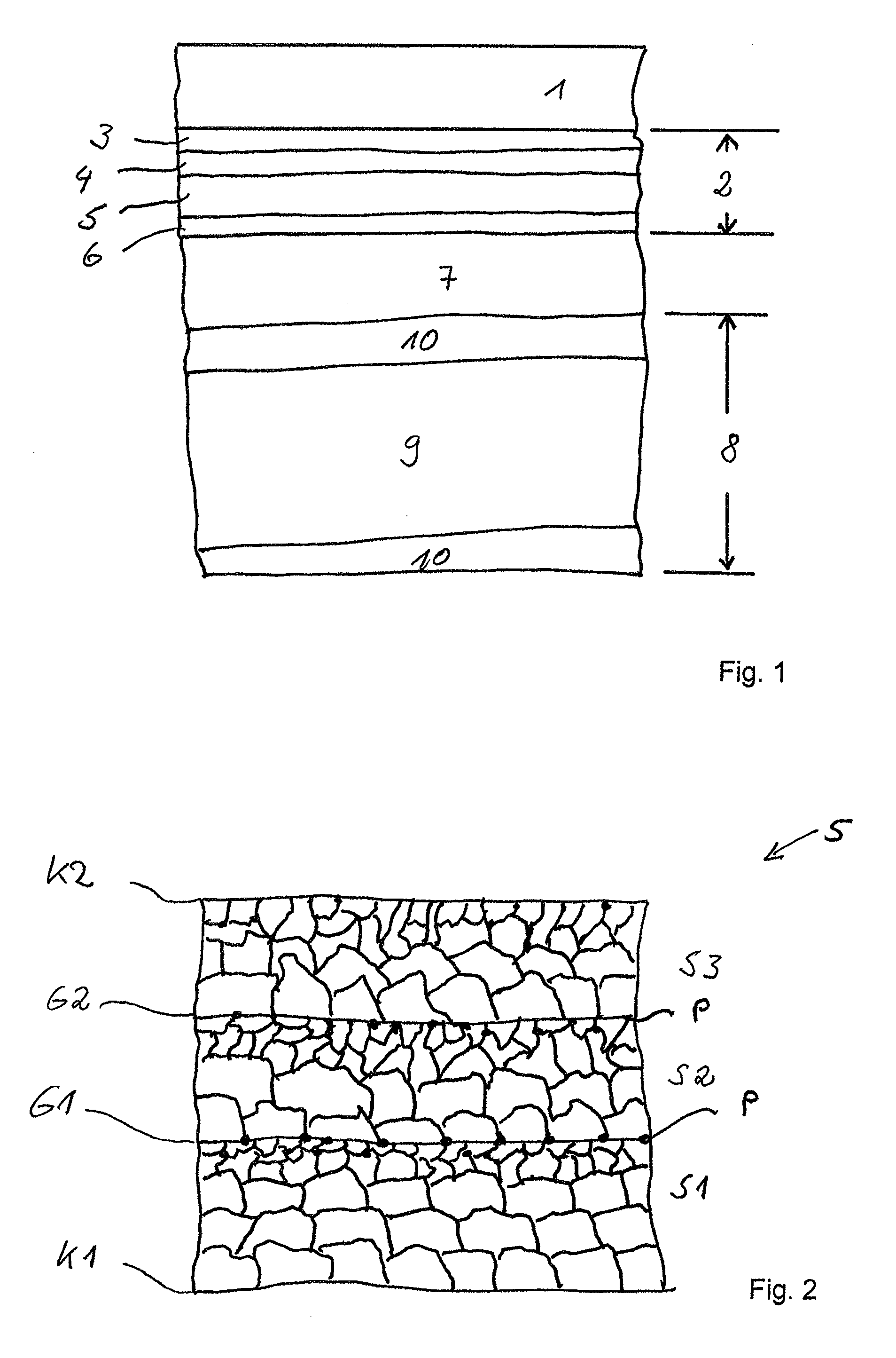
[0024]FIG. 1 shows a stylized cross-sectional view through a DCB substrate with a chip arranged thereon, wherein a soldering paste is provided between the chip and the DCB substrate. A fixed composite assembly of the chip with the DCB substrate can be produced from such an arrangement by supplying heat.

[0025]In FIG. 1, a chip body, designated generally by 1, is produced from Si, for example. A metallization is provided at one side of chip body 1, the metallization being formed from a layer assemblage, designated generally by 2. Layer assemblage 2 consists of a plurality of sequential metallic layers produced by means of a suitable physical coating method, such as PVD or sputtering. A base layer 3 is formed substantially from Al. A first intermediate layer 4 deposited thereon can substantially consist of a TiW alloy. A soldering layer 5 consisting of a plurality of layers (shown in more detail in FIG. 2) is deposited on first intermediate layer 4. Each of the layers can be produced f...


PUM


Abstract

A layer assemblage for a semiconductor chip having a chip body for producing a soldering connection for the chip. The assemblage is provided on a side of a chip body formed from a semiconducting material, wherein the layer assemblage is formed from a plurality of sequential metal layers which follow one above another and are produced by means of a physical coating method, and wherein a solderable soldering layer is provided between a noble metal layer situated at a surface of the layer assemblage and the chip body. In order to avoid an undesired penetration of a solder through the layer assemblage the soldering layer has at least one internal interface formed by an interruption of the coating method.

Description

BACKGROUND OF THE INVENTION[0001]1. Field of the Invention[0002]This invention is directed to a layered metal chip used to produce a soldering connection for a power semiconductor module.[0003]2. Description of the Related Art[0004]Known chips for producing power semiconductor modules are usually soldered onto a support, e.g. a Direct Copper Bonded (“DCB”) substrate or a metallic plate, for heat dissipation purposes. Reference is made to Lugscheider E. et al. “Spannungsreduktion in Chip-DCB-Verbunden mittels Ausnutzung der intrinsischen Spannungseigenschaften von PVD-Metallisierungsschichten” [“Stress reduction in chip-DCB composite assemblies by means of utilization of the intrinsic stress properties of PVD metallization layers”], Verbundwerkstoffe and Werkstoffverbunde [Composite materials and materials composites], M. Schimmerer (ed.), 2005. Soldering connections may furthermore be necessary for producing electrical connections.[0005]In order to produce the soldering connection, ...

Claims


Application Information

Patent Timeline
Patent Type & Authority Patents(United States)
IPC IPC(8): H01L23/48
CPCH01L24/05H01L24/29H01L24/32H01L24/83H01L24/27H01L2924/00013H01L2224/04026H01L2224/32225H01L2224/32245H01L2224/83191H01L2224/83447H01L2224/83801H01L2924/01005H01L2924/01013H01L2924/01015H01L2924/01029H01L2924/01046H01L2924/01047H01L2924/0105H01L2924/01074H01L2924/01075H01L2924/01078H01L2924/01079H01L2924/01327H01L2924/014H01L2924/10329H01L2924/19043H01L2224/05H01L2224/29H01L2224/29298H01L2924/01006H01L2924/01023H01L2924/01024H01L2924/01033H01L2224/29101H01L2924/0132H01L2924/15724H01L2224/29111H01L2924/00H01L2924/01014H01L2924/01032H01L2924/01022H01L2924/01028H01L2924/01031H01L2924/00014H01L2224/29099H01L2224/29199H01L2224/29299H01L2224/2929H01L2924/15747H01L21/56H01L21/64H01L21/67
Inventor BERBERICH, SVEN
Owner SEMIKRON ELECTRONICS GMBH & CO KG
Why Eureka
Try Eureka