Semiconductor device and manufacturing method thereof

a semiconductor and semiconductor technology, applied in the direction of transistors, electroluminescent light sources, electric lighting sources, etc., can solve the problems of increasing transistor cost and danger of depletion, and achieve the effects of stable electric characteristics, reduced transistor threshold voltage, and stable electric characteristics

Active Publication Date: 2013-01-29
SEMICON ENERGY LAB CO LTD
View PDF23 Cites 43 Cited by
  • Summary
  • Abstract
  • Description
  • Claims
  • Application Information

AI Technical Summary

Benefits of technology

[0021]It is an object of an embodiment of the present invention to provide a transistor including an oxide layer which includes Zn and does not include a rare metal such as In or Ga. It is an object of an embodiment of the present invention to reduce variation in the threshold voltage of a transistor including an oxide layer including Zn. Further, it is an object of an embodiment of the present invention to provide the transistor which includes an oxide layer including Zn and a semiconductor device including the transistor. Furthermore, it is an object of an embodiment of the present invention to provide a display device which includes the transistor including the oxide layer.
[0032]According to an embodiment of the present invention, a transistor including an oxide layer which includes Zn and does not include a rare metal such as In or Ga can be provided. According to an embodiment of the present invention, a transistor including an oxide layer including Zn is formed by stacking an oxide semiconductor layer including insulating oxide over an oxide layer so that the oxide layer is overlaps with a source electrode layer or a drain electrode layer with the oxide semiconductor layer including insulating oxide interposed therebetween, whereby variation in the threshold voltage of the transistor can be reduced and electric characteristics can be stabilized. According to an embodiment of the present invention, a semiconductor device including the transistor can be provided.
[0033]By using the transistor for a pixel portion and a driver circuit portion of a display device, the display device can have stable electric characteristics and high reliability.

Problems solved by technology

However, In and Ga in the In—Ga—Zn-based oxide are rare metals and very expensive, which may lead to an increase in transistor cost.
Furthermore, In and Ga resources are in danger of depletion, and from an environment standpoint, discovery of an alternative material is desired.

Method used


Image

  • Semiconductor device and manufacturing method thereof
  • Semiconductor device and manufacturing method thereof
  • Semiconductor device and manufacturing method thereof

Examples


embodiment 1

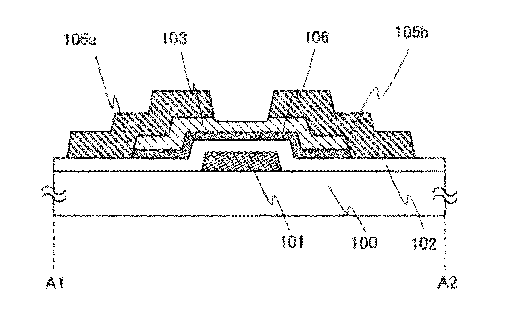
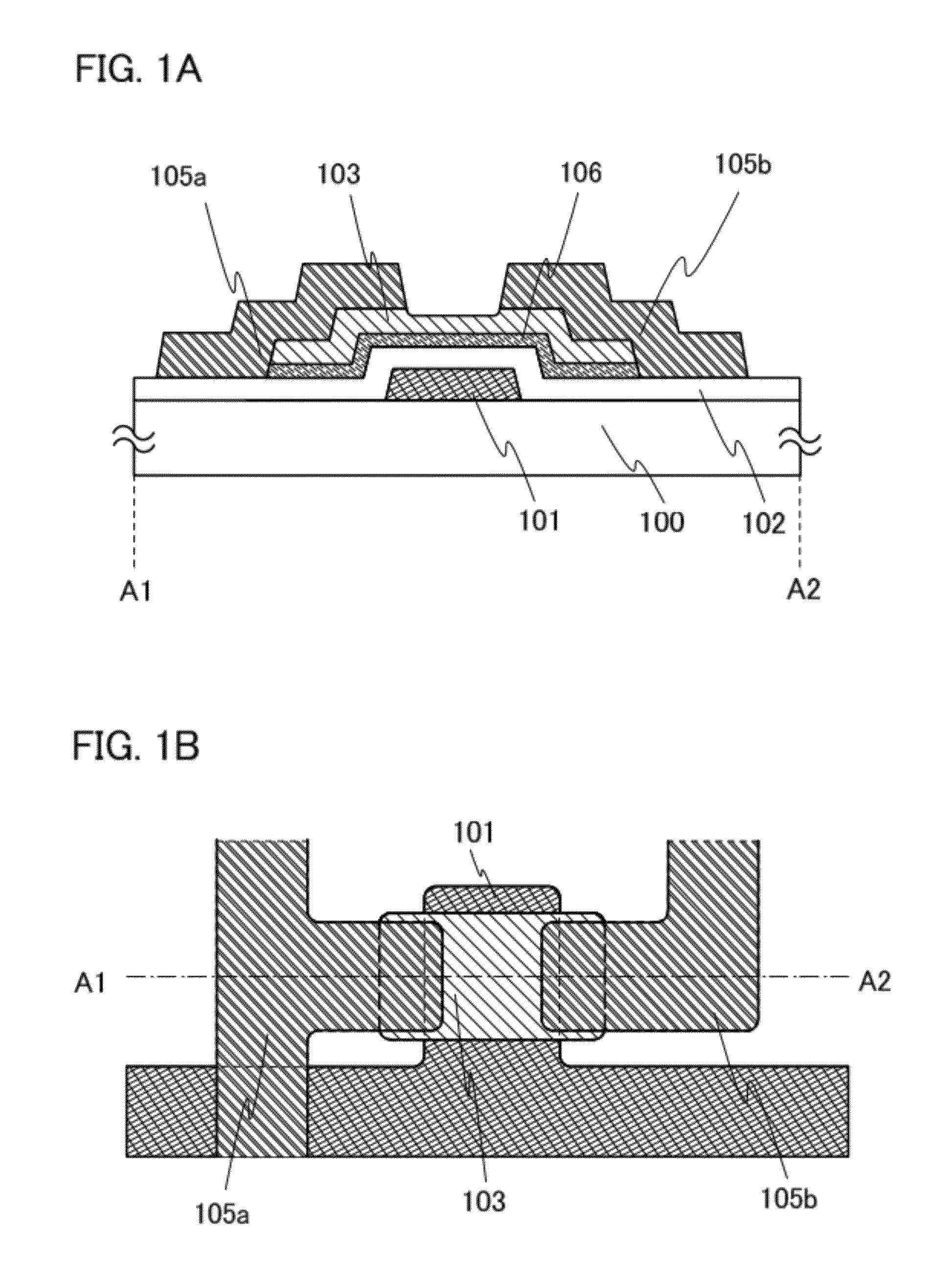
[0079]In this embodiment, a structure of a transistor will be described with reference to FIGS. 1A and 1B.

[0080]A transistor having a bottom gate structure of this embodiment is illustrated in FIGS. 1A and 1B. FIG. 1A is a cross-sectional view, and FIG. 1B is a plan view. FIG. 1A is a cross-sectional view along line A1-A2 of FIG. 1B.

[0081]In the transistor illustrated in FIGS. 1A and 1B, a gate electrode layer 101 is provided over a substrate 100, a gate insulating layer 102 is provided over the gate electrode layer 101, an oxide layer 106 is provided over the gate insulating layer 102, an oxide semiconductor layer 103 including insulating oxide is provided over the oxide layer 106, and source and drain electrode layers 105a and 105b are provided over the oxide semiconductor layer 103 including insulating oxide. Note that the oxide layer 106 and the oxide semiconductor layer 103 including insulating oxide include zinc (Zn).

[0082]The gate electrode layer 101 is formed to have a singl...

embodiment 2

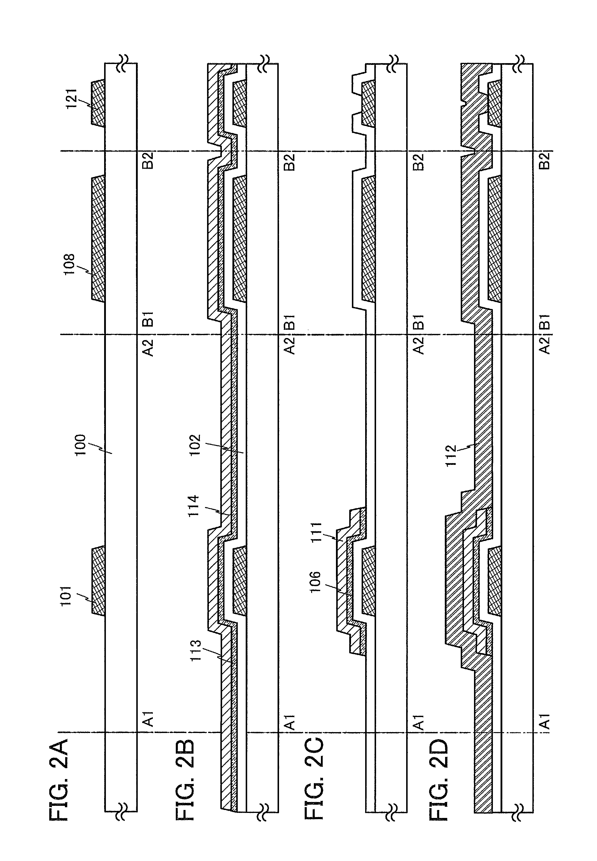
[0127]In this embodiment, a manufacturing process of a display device including the transistor described in Embodiment 1 will be described with reference to FIGS. 2A to 2D, FIGS. 3A to 3C, FIG. 4, FIG. 5, FIG. 6, FIG. 7, FIG. 8, and FIGS. 9A-1, 9A-2, 9B-1, and 9B-2. FIGS. 2A to 2D and FIGS. 3A to 3C are cross-sectional views, and FIG. 4, FIG. 5, FIG. 6, FIG. 7, and FIG. 8 are plan views. Line A1-A2 and Line B1-B2 in FIG. 4, FIG. 5, FIG. 6, FIG. 7, and FIG. 8 correspond to Line A1-A2 and Line B1-B2 in the cross-sectional views of FIGS. 2A to 2D and FIGS. 3A to 3C.

[0128]First, a substrate 100 is prepared. As the substrate 100, the following can be used: an alkali-free glass substrate manufactured by a fusion method or a floating method, such as a barium borosilicate glass substrate, an aluminoborosilicate glass substrate, or an aluminosilicate glass substrate; a ceramic substrate; a heat-resistant plastic substrate that can resist process temperature of this manufacturing process; or ...

embodiment 3

[0192]In this embodiment, a transistor having a structure different from the transistor described in Embodiment 1 will be described with reference to FIGS. 31A and 31B.

[0193]FIGS. 31A and 31B illustrate a transistor having a bottom gate structure of this embodiment. In the transistor illustrated in FIGS. 31A and 31B, the gate electrode layer 101 is provided over the substrate 100, the gate insulating layer 102 is provided over the gate electrode layer 101, the oxide layer 106 is provided over the gate insulating layer 102, the oxide semiconductor layer 103 including insulating oxide is provided over the oxide layer 106, buffer layers 301a and 301b are provided over the oxide semiconductor layer 103 including insulating oxide, and the source and drain electrode layers 105a and 105b are provided over the buffer layers 301a and 301b. Note that the oxide layer 106 and the oxide semiconductor layer 103 including insulating oxide include zinc (Zn). That is, the transistor illustrated in F...


PUM


Abstract

An object is to provide a transistor including an oxide layer which includes Zn and does not include a rare metal such as In or Ga. Another object is to reduce an off current and stabilize electric characteristics in the transistor including an oxide layer which includes Zn. A transistor including an oxide layer including Zn is formed by stacking an oxide semiconductor layer including insulating oxide over an oxide layer so that the oxide layer is in contact with a source electrode layer or a drain electrode layer with the oxide semiconductor layer including insulating oxide interposed therebetween, whereby variation in the threshold voltage of the transistor can be reduced and electric characteristics can be stabilized.

Description

BACKGROUND OF THE INVENTION[0001]1. Field of the Invention[0002]The present invention relates to a semiconductor device including an oxide semiconductor, a display device including the semiconductor device, and a manufacturing method thereof.[0003]2. Description of the Related Art[0004]There are a wide variety of metal oxides and such metal oxides are used for various applications. Indium oxide is a well-known material and is used as a light-transmitting electrode material which is necessary for liquid crystal displays and the like.[0005]Some metal oxides have semiconductor characteristics. As metal oxides having semiconductor characteristics, for example, there are tungsten oxide, tin oxide, indium oxide, zinc oxide, and the like, and a transistor having such a metal oxide having semiconductor characteristics in its channel formation region has been proposed (Patent Documents 1 to 4, Non-Patent Document 1).[0006]As metal oxides, multi-component oxides as well as single-component ox...

Claims


Application Information

Patent Timeline
Patent Type & Authority Patents(United States)
IPC IPC(8): H01L29/786H05B44/00
CPCH01L27/12H01L27/1225H01L27/1255H01L29/78618H01L29/7869H01L29/78696H01L29/66969H01L29/78609H01L21/02554H01L21/02565H01L29/45
Inventor YAMAZAKI, SHUNPEIGODO, HIROMICHIKISHIDA, HIDEYUKI
Owner SEMICON ENERGY LAB CO LTD
Why Eureka
Try Eureka