Supply-regulated VCO architecture

a supply regulation and vco technology, applied in the field of phaselocked loops (plls), can solve the problems of limiting the stability of the supply regulation loop, the amount of integrated circuit area required, and the noise on the supply voltage vdd_noisy, so as to increase the capacitance of the bypass capacitor without affecting the stability of the overall pll loop, the effect of reducing the noise sensitivity of the supply voltag

Active Publication Date: 2013-01-29
QUALCOMM INC
View PDF11 Cites 31 Cited by
  • Summary
  • Abstract
  • Description
  • Claims
  • Application Information

AI Technical Summary

Benefits of technology

[0014]In a first novel aspect, an auxiliary supply current circuit supplies an auxiliary supply current IASUP to the oscillator, thereby reducing the amount of supply current ICL a supply regulation control loop circuit must supply to control the oscillator. Because the amount of supply current ICL that the supply regulation control loop circuit must supply is reduced, a transistor in the supply regulation control loop circuit through which the supply current ICL is supplied can be reduced in size. By reducing the size of this transistor, parasitics that give rise to a pole (at frequency F1) in the supply regulation loop are reduced. Reducing parasitics in this transistor increases the frequency F1 of this pole and allows the designer to compensate the supply regulation loop by treating the pole due to the bypass capacitor at F2 as the dominant pole. The capacitance of the bypass capacitor can be increased without adversely affecting loop stability. This serves to reduce peaking in the supply sensitivity transfer function VS(s)VDD_NOISY(s).
[0017]In a second novel aspect, a supply regulation control loop circuit supplies a control current to a master oscillator. The output of the master oscillator is then used to close a PLL control loop. The bypass capacitor of the supply-regulated VCO is not, however, coupled to the supply current input lead of this master oscillator but rather is coupled to a slave oscillator. The output of the slave oscillator is then used to clock the external circuits such as a CPU or an RF synthesizer or another circuit. The slave oscillator is injection-locked to the master oscillator. Because the bypass capacitor is outside the main PLL feedback control loop, the capacitance of the bypass capacitor can be increased without affecting the stability of the main PLL loop. Supply noise sensitivity can now be minimized by increasing the capacitance of the bypass capacitor without affecting overall PLL loop stability. If the bypass capacitor were provided across the master oscillator, then it would introduce a pole in the PLL loop transfer function at frequency=½π(RVCO*CBYCAP) where RVCO is the effective resistance of the master oscillator and CBYCAP is the value of the bypass capacitor. Because the bypass capacitor is outside the main PLL feedback control loop, the capacitance CBYCAP of the bypass capacitor is limited only by integrated circuit area constraints.

Problems solved by technology

Unfortunately, there is often noise on the supply voltage VDD_NOISY at supply voltage conductor 18.
One limit on how low F2 can be is the amount of integrated circuit area required to realize a larger bypass capacitor.
Another limit is stability of the supply regulation loop.
Another problem associated with the circuit of FIG. 3 is that the low frequency noise (such as 1 / f noise) from the replica transistors themselves 26 and 27 will cause low frequency variations in ICTRL.
However, the corrective voltage applied to gate of transistor M2 will actually cause undesirable low frequency variations in ICTRL.
This is a problem only at frequencies within the bandwidth of the supply regulation control loop 5.

Method used


Image

  • Supply-regulated VCO architecture
  • Supply-regulated VCO architecture
  • Supply-regulated VCO architecture

Examples


Embodiment Construction

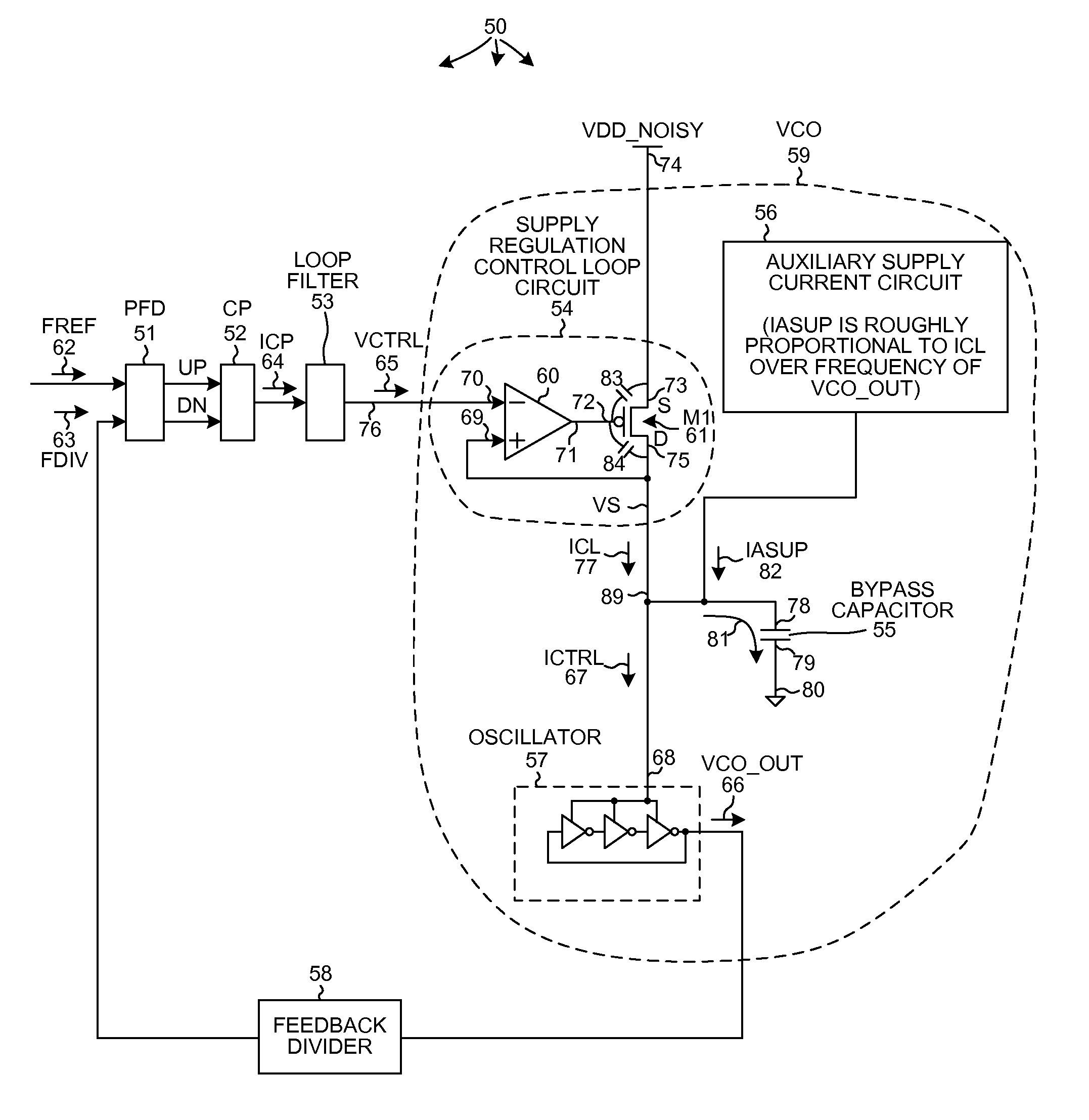
[0034]FIG. 6 is a diagram of a Phase-Locked Loop (PLL) 50 involving a supply-regulated VCO 59 in accordance with a first novel aspect. PLL 50 includes a Phase-to-Frequency Detector (PFD) 51, a Charge Pump (CP) 52, a loop filter 53, a supply regulation control loop circuit 54, a bypass capacitor 55, an auxiliary supply current circuit 56, an oscillator 57, and a feedback divider 58. The supply regulation control loop circuit 54, the oscillator 57, and the bypass capacitor 55 together form the supply-regulated VCO 59.

[0035]PFD 51 compares the phase of a reference signal FREF 62 and the phase of a feedback signal FDIV 63 and outputs UP pulses or DN pulses depending on whether the phase of FDIV leads or leads or lags the phase of FREF. Charge pump 52 converts the pulses into a control current signal ICP 64. Control signal ICP 64 is filtered by loop filter 53 and is converted into a control voltage signal VCTRL 65. The VCTRL signal is sometimes referred to as a fine tune signal and is de...


PUM


Abstract

A supply-regulated VCO exhibits reduced or no supply sensitivity peaking. The VCO includes an oscillator whose supply current is regulated to control the oscillating frequency of the oscillator. A VCO input signal controls the supply current so that there is a relationship between the input signal and the oscillator output frequency. Power supply noise that might otherwise affect oscillator operation is shunted from a supply current input lead of the oscillator to ground by a bypass capacitor. In one example, an auxiliary circuit supplies an auxiliary supply current to the oscillator, thereby reducing the amount of supply current a supply regulation control loop circuit must supply. In another example, a supply regulation control loop circuit supplies a control current to a main oscillator, but the bypass capacitor is not coupled to this oscillator but rather is coupled to a slave oscillator that is injection locked to the main oscillator.

Description

BACKGROUND INFORMATION[0001]1. Technical Field[0002]The present disclosure relates to Phase-Locked Loops (PLLs) that make use of a supply-regulated Voltage-Controlled Oscillator (VCO) architecture.[0003]2. Background Information[0004]A supply-regulated Phase-Locked Loop (PLL) generally involves a Voltage-Controlled Oscillator (VCO) whose oscillating frequency is determined and controlled by an input control signal such as a control voltage signal. FIG. 1 (Prior Art) is a diagram of one such PLL 1. PLL 1 involves a Phase-to-Frequency Detector (PFD) 2, a Charge Pump (CP) 3, a loop filter 4, a supply regulation control loop circuit 5, a bypass capacitor 6, an oscillator 7, and a feedback divider 8. The supply regulation control loop circuit 5, the oscillator 7, and the bypass capacitor 6 together form a VCO 9. Supply regulation control loop circuit 5 involves an operational amplifier 10 and a P-channel field effect transistor M111 interconnected as illustrated. PFD 2 compares the phase...

Claims


Application Information

Patent Timeline
Patent Type & Authority Patents(United States)
IPC IPC(8): H03L1/00H03L7/099H03K3/03
CPCH03L7/0805H03L7/24H03L7/0995H03L7/099
Inventor RAGHUNATHAN, ASHWINPEDRALI-NOY, MARZIOWADHWA, SAMEER
Owner QUALCOMM INC
Why Eureka
Try Eureka