Semiconductor device and method having trenches in a drain extension region

a technology of drain extension and semiconductor devices, which is applied in the direction of semiconductor devices, basic electric elements, electrical appliances, etc., can solve the problems of limiting the applicability of semiconductor devices to specific application domains, increasing the footprint of semiconductor devices to meet performance requirements, etc., and achieves the effect of not compromising the performance of semiconductor devices and being more reliabl

Active Publication Date: 2013-02-12
NXP BV
View PDF8 Cites 4 Cited by
  • Summary
  • Abstract
  • Description
  • Claims
  • Application Information

AI Technical Summary

Benefits of technology

[0012]In an embodiment, the distance between the third region and said boundaries does not exceed the width of an active stripe, which ensures that the performance of the semiconductor device is not compromised, and in fact even can improve, by the presence of a substrate portion between the p-n junction of the third region and the active stripes on the one side and the shallow trenches on the other side.
[0014]In a further embodiment, the dielectric comprises a void separating a first layer region across the third region from a second layer region across the trenches and active stripes, said void overlapping the boundaries between the respective substrate portions and said trenches. This has the advantage that the control over the distance from the third region to the trench is less critical in terms of device performance because the high electric field is shifted away from the control terminal formed over the third region, e.g. a gate or a base terminal, towards a dummy control terminal comprising the second layer portion by the dummy control terminal potential. In addition, the dummy effect drives the current through the device to a greater depth, thus making the device more reliable because the number of hot carriers injected into the dielectric is reduced.
[0016]The semiconductor device of the present invention may be incorporated in an integrated circuit (IC). Such an IC benefits from the relatively small footprints of the semiconductor devices of the present invention, such that a high voltage portion of the IC can be realized whilst requiring limited silicon area, thus limiting the overall size and cost of the IC. Non-limiting examples of suitable applications include dc-dc converters, power management units and display drivers.

Problems solved by technology

Although in some of the devices of WO2006 / 136979 this problem has been avoided by extending the shallow trenches through the third region such as a channel region into the first region such as the source region, these devices suffer from a lower current drive, which means that the footprint of these devices must be increased to meet their performance requirements, which is also unwanted, and in fact limits the applicability of these devices to specific application domains only.

Method used


Image

  • Semiconductor device and method having trenches in a drain extension region
  • Semiconductor device and method having trenches in a drain extension region
  • Semiconductor device and method having trenches in a drain extension region

Examples


Embodiment Construction

[0020]Embodiments of the invention are described in more detail and by way of non-limiting examples with reference to the accompanying drawings, wherein

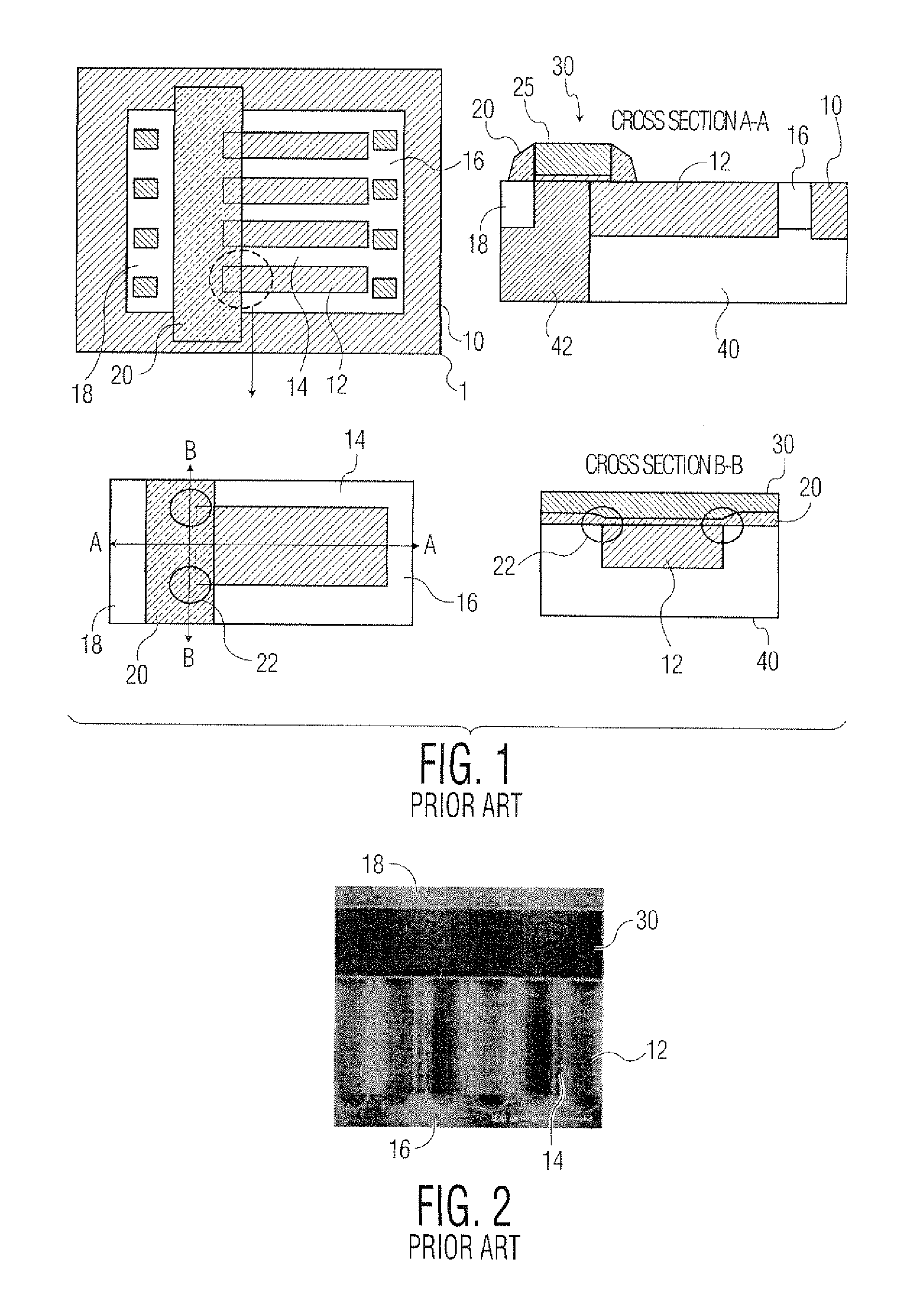
[0021]FIG. 1 schematically depicts a prior art semiconductor device;

[0022]FIG. 2 schematically depicts a detail of the prior art semiconductor device;

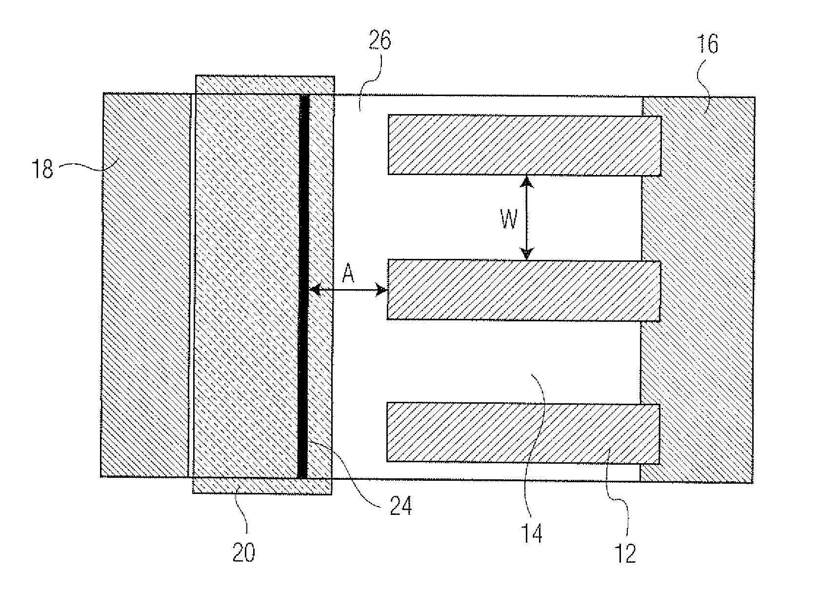
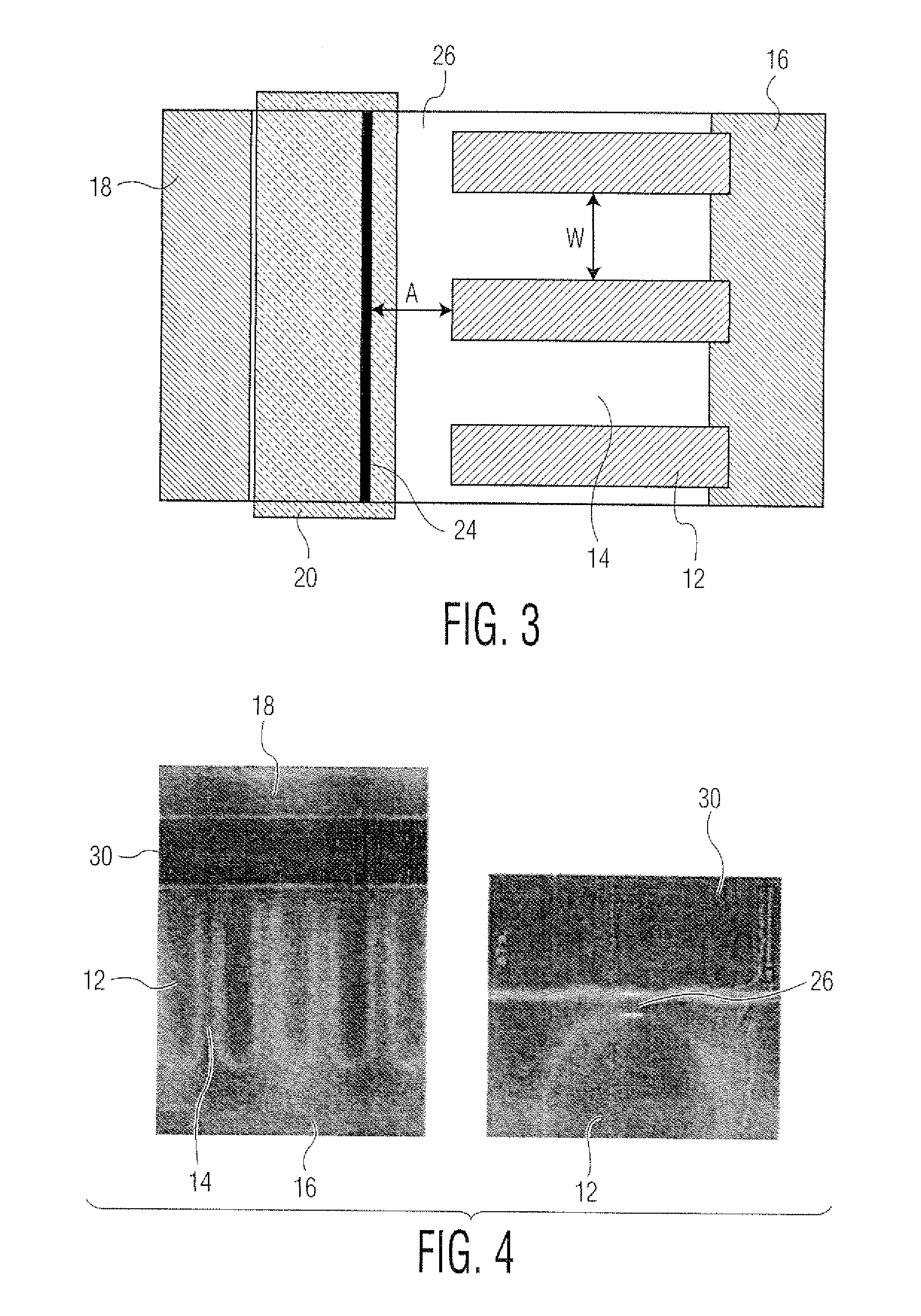
[0023]FIG. 3 schematically depicts a semiconductor device in accordance with an embodiment of the present invention;

[0024]FIG. 4 schematically depicts a detail of the semiconductor device in accordance with an embodiment of the present invention;

[0025]FIG. 5 schematically depicts the off-state characteristics of the prior art semiconductor device and a semiconductor device of the present invention;

[0026]FIG. 6 schematically depicts a semiconductor device in accordance with another embodiment of the present invention;

[0027]FIG. 7 schematically depicts an electrical field profile of the prior art semiconductor device and a semiconductor device of the present invention; and

[0028]FIG. 8 sch...


PUM


Abstract

A semiconductor device comprises a substrate including a first region and a second region of a first conductivity type and a third region between the first and second regions of a second conductivity type opposite to the first conductivity type, and being covered by a dielectric layer. A plurality of trenches laterally extend between the third and second region, are filled with an insulating material, and are separated by active stripes with a doping profile having a depth not exceeding the depth of the trenches wherein each trench terminates before reaching the dielectric layer and is separated from the third region by a substrate portion such that the respective boundaries between the substrate portions and the trenches are not covered by the dielectric layer. A method for manufacturing such a semiconductor device is also disclosed.

Description

FIELD OF THE INVENTION[0001]The present invention relates to a semiconductor device comprising a substrate including a first region and a second region doped with a dopant of a first conductivity type and a third region between the first region and the second region doped with a dopant of a type opposite to the first conductivity type, the third region being covered by a dielectric layer, the substrate further comprising a plurality of trenches laterally extending between the first region and the second region, said trenches being filled with an insulating material and having a predetermined depth, and being separated by active stripes comprising a doping profile having a depth not exceeding the predetermined depth.[0002]The present invention further relates to a method of manufacturing such a semiconductor device.BACKGROUND OF THE INVENTION[0003]In semiconductor devices including p-n junctions, including for example simple diodes as well as more complex devices such as field effect...

Claims


Application Information

Patent Timeline
Patent Type & Authority Patents(United States)
IPC IPC(8): H01L29/66H01L21/76
CPCH01L29/0653H01L29/0692H01L29/66659H01L29/7835H01L29/42364H01L29/4238H01L29/402
Inventor SONSKY, JANHERINGA, ANCO
Owner NXP BV
Why Eureka
Try Eureka