Electronic circuit device

a technology of electronic circuit and electrode, which is applied in the direction of semiconductor devices, diodes, electrical apparatus, etc., can solve the problems of inevitably forming high-density interface levels, oxide films formed over silicon carbide substrates, and remaining carbon in oxide films, etc., to facilitate the formation of p-type and n-type conductivities

Inactive Publication Date: 2013-03-05
RENESAS ELECTRONICS CORP
View PDF5 Cites 1 Cited by
  • Summary
  • Abstract
  • Description
  • Claims
  • Application Information

AI Technical Summary

Benefits of technology

[0009]In general, semiconductor elements for high power applications of several watts or greater are called “power semiconductor elements”. In the power semiconductor elements, on resistance and breakdown voltage are in a trade-off relationship defined by a band gap of a substrate material. It is therefore effective to use a substrate material having a band gap greater than that of silicon in order to exceed the performance of a silicon (Si) element widely used as the power semiconductor element. In particular, silicon carbide (SiC) has attracted a lot of attention because it can realize a high performance semiconductor element such as MISFET (metal insulator semiconductor field effect transistor) by making use of its characteristics that it has a band gap about three times as much as that of silicon, it facilitates formation of both p type and n type conductivities, and it can form an oxide film through thermal oxidation.
[0013]Such a junction FET using silicon carbide as a base material enables to realize a high-performance normally-off type element not susceptible to the interface of an oxide film.
[0018]An object of the invention is to provide a silicon carbide semiconductor device easy to use and a manufacturing method of the device.
[0023]In short, in the invention, a voltage applied to the external terminal of a gate is shared by a capacitive component coupled to a gate electrode and a gate capacitance of a junction FET, making it possible to apparently decrease the gate voltage dependence of a drain current, thereby facilitating the control of the gate of the junction FET.

Problems solved by technology

An oxide film formed over a silicon carbide substrate has a significant problem, that is, remaining of carbon in the oxide film when silicon carbide is thermally oxidized inevitably forms a high-density interface level.
This causes considerable deterioration in channel mobility and a marked increase in the on resistance of the MISFET.
In addition, carbon in the oxide film also causes deterioration in reliability of the oxide film and becomes a huge barrier against realizing the MISFET.
In general, normally-off type power semiconductor elements are desired because normally-on type ones are limited in their use in view of fail safe.

Method used


Image

  • Electronic circuit device
  • Electronic circuit device
  • Electronic circuit device

Examples


first embodiment

[0091]1. Description of a Semiconductor Device and the Like of the Present Application (Mainly, from FIG. 1 to FIG. 9)

[0092]In this section, only an essential part of a normally-off type silicon carbide-based junction FET (1) is illustrated to mainly make a fundamental description. A peripheral structure and a manufacturing method of it will be described in Sections 7 and 8.

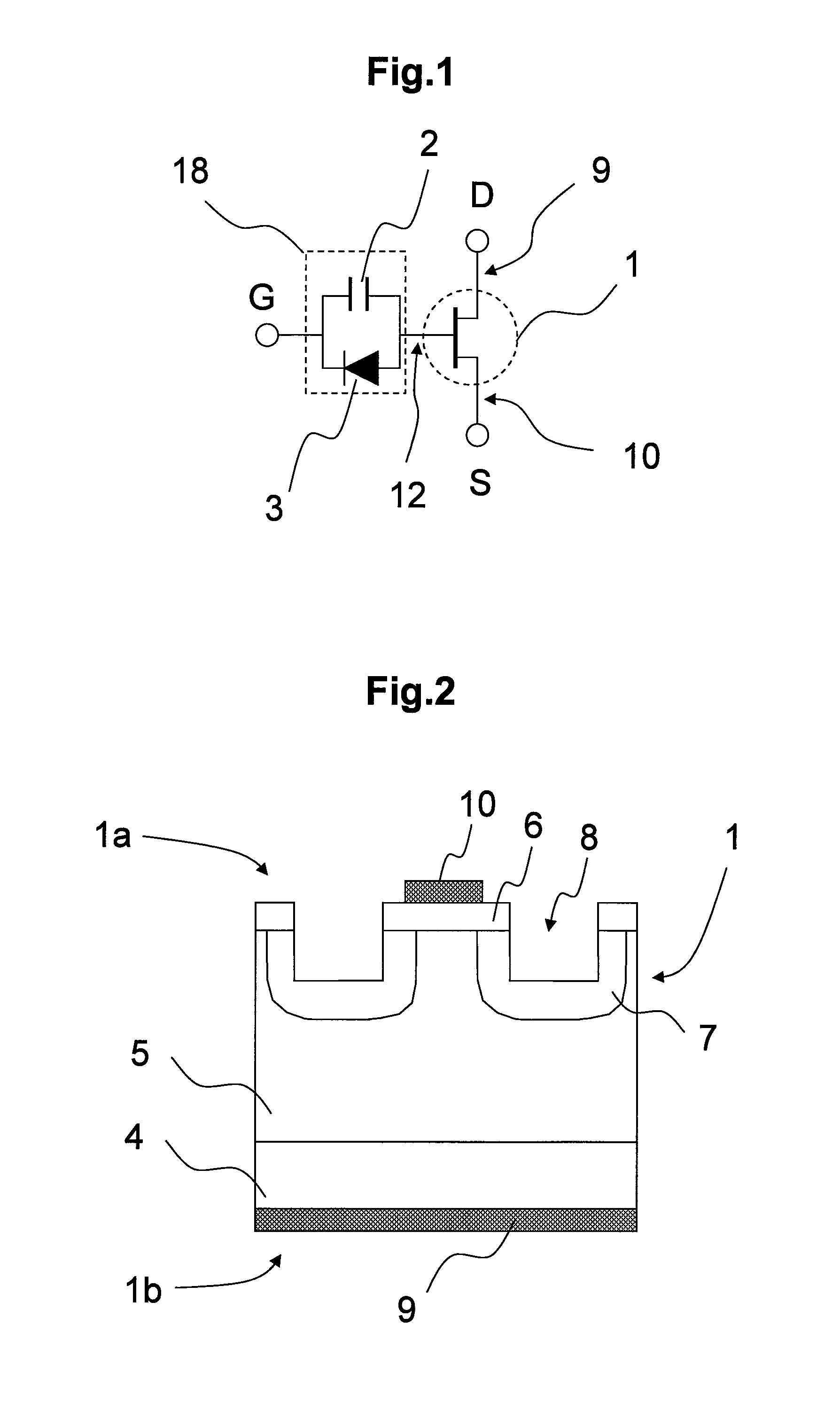
[0093]The first embodiment of the invention will hereinafter be described referring to some drawings. FIG. 1 is an equivalent circuit diagram of the first embodiment of the invention; and FIGS. 2 and 3 are a cross-sectional structural view of a silicon carbide junction FET to be used in the present embodiment and a characteristic diagram of a gate. As illustrated in FIG. 1, no additional element is inserted between an external source terminal S of the silicon carbide-based junction FET (1) and a source electrode 10 and an external drain terminal D and a drain electrode 9. As an insertion element or element group ...

second embodiment

[0101]2. Description of a Semiconductor Device and the Like of a Second Embodiment According to the Present Application (Mainly from FIG. 10 to FIG. 13)

[0102]FIG. 10 is a circuit diagram of the second embodiment of the invention. A difference from the first embodiment is that a diode 3 serves also as a capacitive component instead of the capacitor 2. Accordingly, the capacitance of the diode 3 becomes one digit greater than that of the first embodiment. A silicon carbide junction FET is similar to that of the first embodiment.

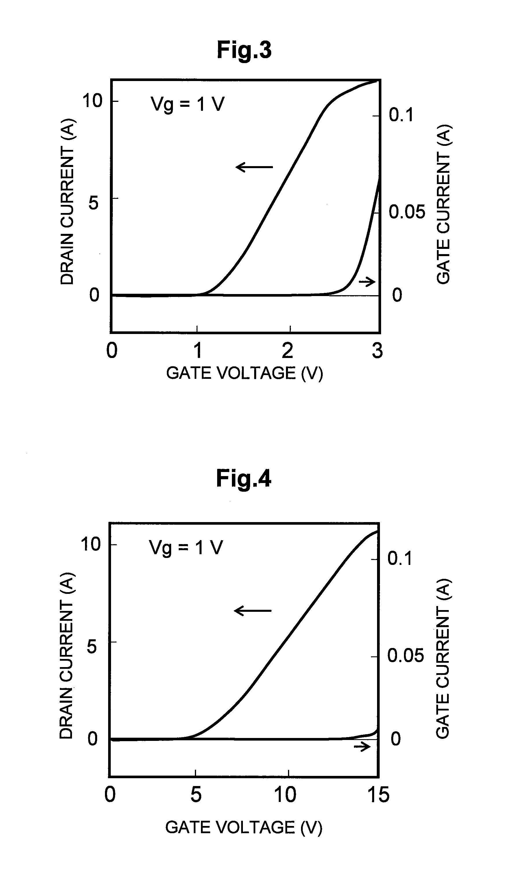
[0103]Advantages of the present embodiment will next be described. FIG. 11 shows the relationship between a voltage VG of an external gate terminal and a drain current of the junction FET 1. As shown in this graph, the voltage applied to the external gate terminal G is shared by the diode 3 and the gate of the junction FET 1. Application of a voltage of about 2V to the external gate terminal produces a drain current through the junction FET 1, while application...

third embodiment

[0108]3. Description of a Semiconductor Device and the Like of the Present Application (Mainly from FIG. 14 to FIG. 21)

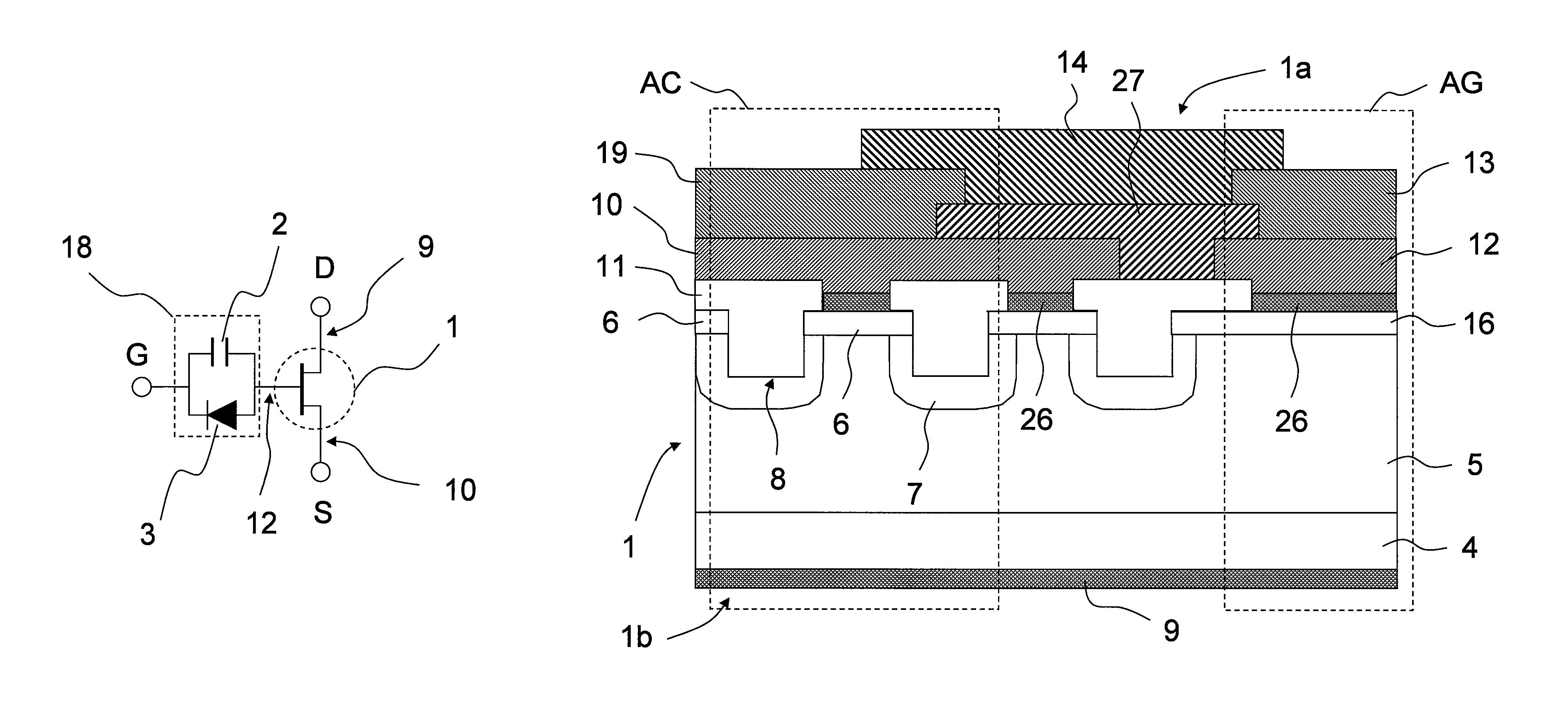
[0109]A difference of the third embodiment from the first embodiment and the second embodiment is that the semiconductor device of the present embodiment includes, in a chip thereof, a capacitor 2 and a diode 3. Prior to describing the present embodiment, the configuration of a conventional chip and the structure of a gate pad will be described referring to FIGS. 14 and 15 (an A-A′ cross-section of a peripheral region of a gate pad illustrated in FIG. 14). In the conventional junction FET 1, a gate pad 13 and a source pad 19 are placed over the surface of the chip and the source pad 19 has an active region 28 of the device right below the source pad 19. An interconnect 12 of the gate is placed over an on-substrate insulating film 11 and is coupled to the gate pad 13. A passivation film 14 is formed to cover therewith the gate pad 13.

[0110]In the present embodiment, ...


PUM


Abstract

A normally-off type silicon carbide junction FET has a problem that the gate thereof is not easy to use due to inferiority in the characteristics of it. This problem occurs because in order to achieve normally-off, the gate voltage should be off at 0V and at the same time, the ON-state gate voltage should be suppressed to about 2.5V to prevent the passage of an electric current through a pn junction between gate and source. Accordingly, a range from the threshold voltage to the ON-state gate voltage is only from about 1 V to 2V and it is difficult to control the gate voltage. Provided in the present invention is an electronic circuit device obtained by coupling, to a gate of a normally-off type silicon carbide junction FET, an element having a capacitance equal to or a little smaller than the gate capacitance of the junction FET.

Description

CROSS-REFERENCE TO RELATED APPLICATIONS[0001]The present application claims priority from Japanese patent application JP 2010-055410 filed on Mar. 12, 2010, the content of which is hereby incorporated by reference into this application.BACKGROUND[0002]The present invention relates to a switching device using silicon carbide as a base material and a gate drive circuit for the switching device.[0003]Japanese Patent Laid-Open No. 2004-134547 (Patent Document 1) or U.S. Patent Laid-Open No. 2005-218424 (Patent Document 2) corresponding thereto discloses an example of a normally-off type silicon carbide junction FET.[0004]Japanese Patent Laid-Open No. 2009-21461 (Patent Document 3) or U.S. Patent Laid-Open No. 2009-14719 (Patent Document 4) corresponding thereto discloses an example of a silicon carbide junction FET having a gate coupled to forward and backward diodes.Patent Documents[0005][Patent Document 1] Japanese Patent Laid-Open No. 2004-134547[0006][Patent Document 2] U.S. Patent ...

Claims


Application Information

Patent Timeline
Patent Type & Authority Patents(United States)
IPC IPC(8): H01L29/24
CPCH01L21/8213H01L27/0629H01L24/05H01L29/66909H01L29/8083H01L29/868H01L29/1608H01L2924/13062H01L2924/12032H01L2224/48195H01L2924/1306H01L2924/13091H01L2224/49111H01L2224/48247H01L2224/48137H01L2224/48091H01L2224/0603H01L2224/02166H01L2224/05556H01L2224/04042H01L2924/00014H01L2924/00H01L2924/12031H01L24/29H01L24/32H01L24/48H01L24/49H01L24/73H01L2224/05624H01L2224/32245H01L2224/73265H01L2924/10253H01L2924/10272H01L2224/29101H01L2924/15788H01L2924/12036H01L2924/14H01L2924/181H01L2224/45099H01L2924/014H01L2924/00012
Inventor SHIMIZU, HARUKAYOKOYAMA, NATSUKI
Owner RENESAS ELECTRONICS CORP
Why Eureka
Try Eureka