Coating/developing device and method

a technology of developing device and coating, which is applied in the direction of photosensitive materials, cleaning using liquids, instruments, etc., can solve the problems of large occupancy area, increased processing burden, and large processing space occupied by processing block, so as to suppress the deterioration of throughput, save processing block space, and efficiently use

Active Publication Date: 2013-04-02
TOKYO ELECTRON LTD
View PDF18 Cites 6 Cited by
  • Summary
  • Abstract
  • Description
  • Claims
  • Application Information

AI Technical Summary

Benefits of technology

[0011]It is, therefore, an object of the present invention to provide a coating / developing device and method capable of operating appropriately by correspondingly responding to the case where the BARC is formed on the top and the bottom of the resist film and the case where the BARC is not formed and further saving the space thereof. Further, it is an object of the present invention to provide a coating / developing device and method capable of suppressing the deterioration of the throughput even when there occurs a trouble in any one of the coating unit blocks.
[0019]In accordance with the present invention, since there are provided the stacked coating unit blocks each of which includes the coating unit, the first BARC forming unit and the second BARC coating unit, each of the coating unit blocks can properly operate by correspondingly responding to a case where the BARC is either formed or not on the top and the bottom of the resist film while saving the space occupied by the processing block. Accordingly, the space can be efficiently used.
[0020]Further, even when there occurs an abnormality in any one of the coating unit blocks, the coating film can be formed by using the other coating unit blocks. Therefore, the overall apparatus need not be stopped, thereby suppressing the deterioration of the throughput compared with a case where the overall apparatus is stopped. In addition, the number of the wafers W remaining in the unit block where the abnormality occurs becomes small by distributing the coating works to the plural coating unit blocks, thereby decreasing the burden of processing the substrates in order to recycle them.

Problems solved by technology

In this case, if the coating unit and the developing unit are provided in a same processing block, the number of units provided in a single processing block becomes great and the size of the processing block is increased, thereby resulting in a large occupancy area thereof.
Further, there may occur a trouble such as a case where the modules such as the coating unit 13A and the heating unit or the transfer units 15A and 15B provided in the processing block 1B become out of order, or the wafer W cannot be transferred at a desired time between the transfer units 15A and 15B and the respective modules.
As a result, the burden of the processing such as a cleaning process, which should be performed to recycle the wafers W, becomes greater.
Moreover, the device cannot be operated while retrieving the wafers W, operating for confirming the locations where the trouble occurs and performing a maintenance work, thereby deteriorating the throughput thereof.
Even in such an arrangement, there may also occur the aforementioned trouble such as the malfunction of the modules and the transfer units in the coating areas and the developing area; however, Japanese Patent Laid-open Publication No. 3337677 does not disclose any approach therefor.

Method used


Image

  • Coating/developing device and method
  • Coating/developing device and method
  • Coating/developing device and method

Examples


Embodiment Construction

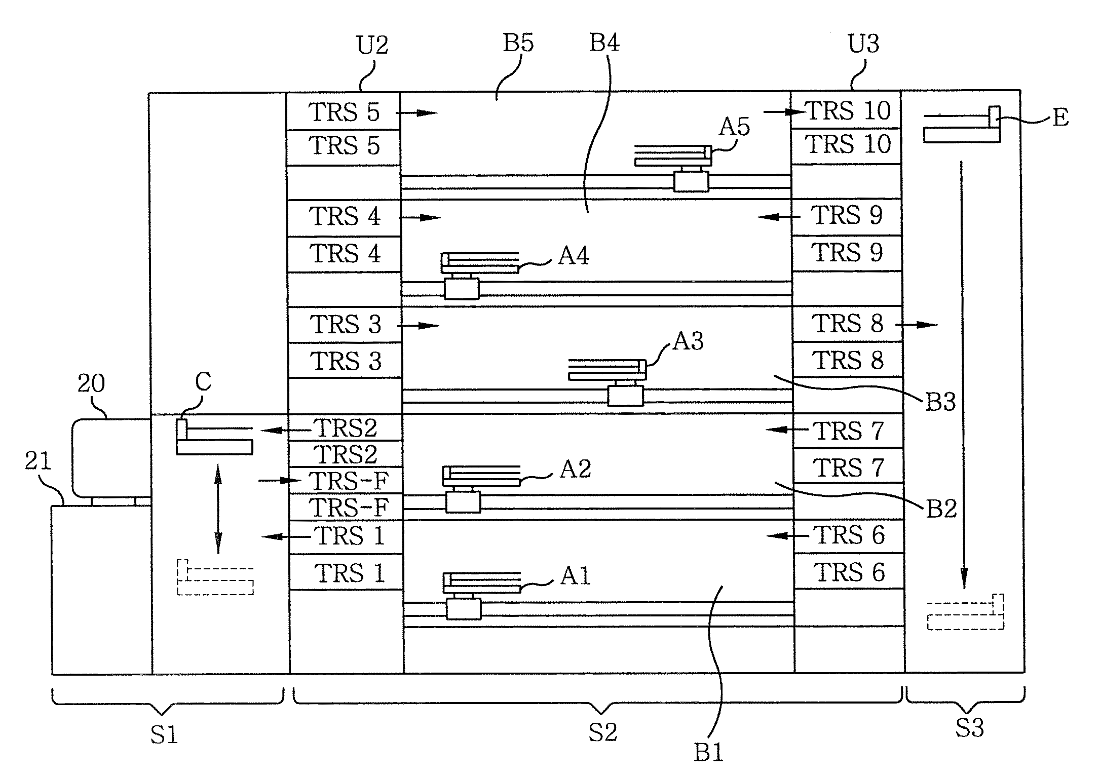
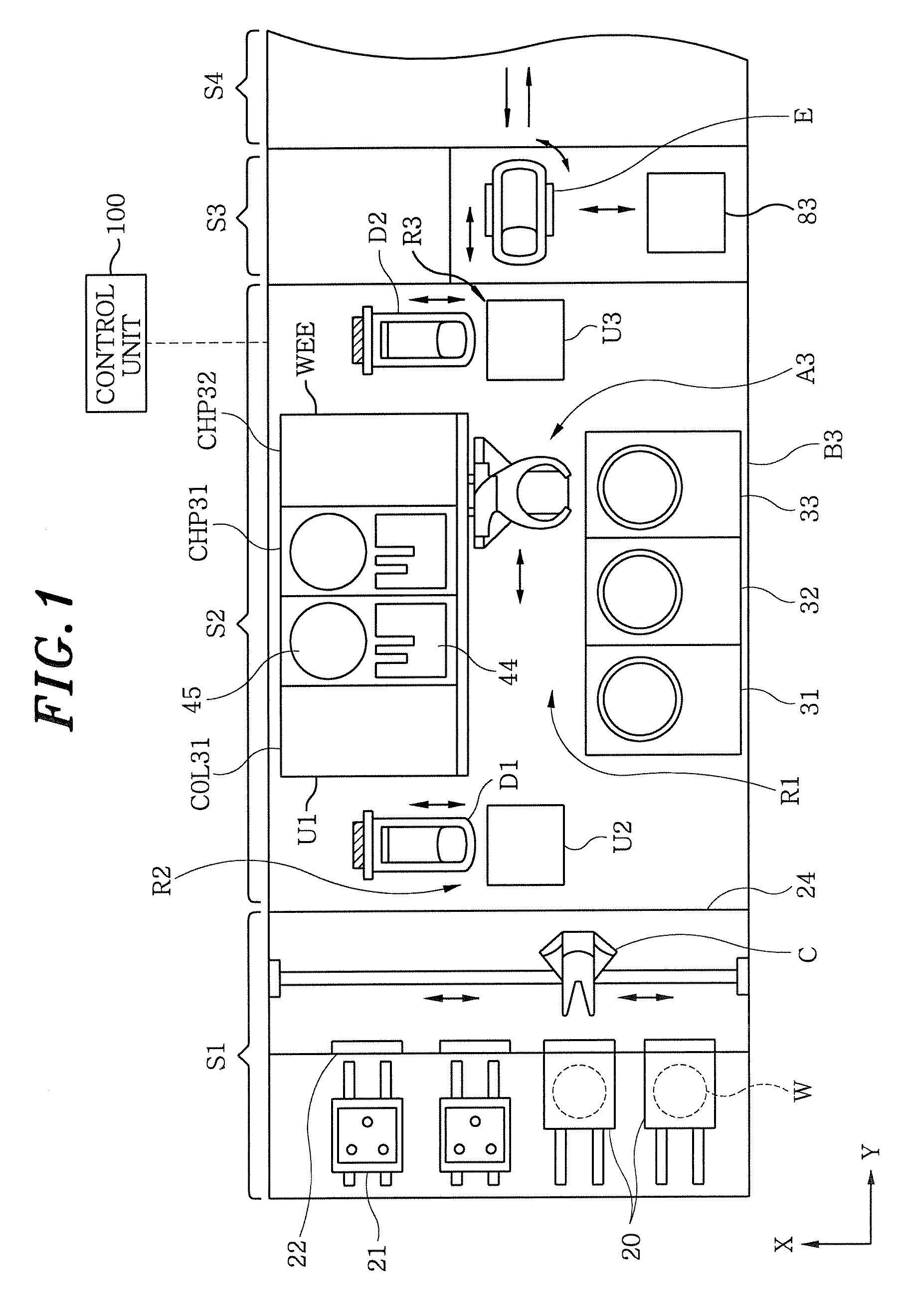
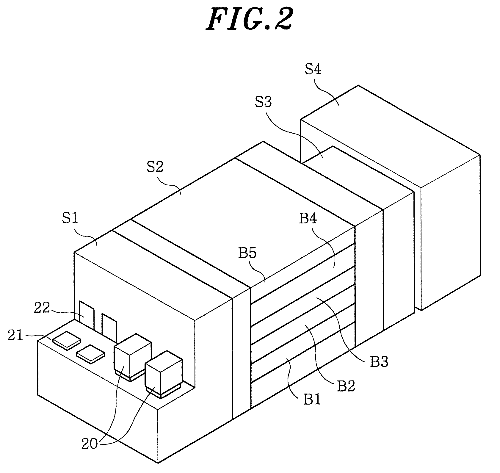
[0034]Hereinafter, there will be described a coating / developing device in accordance with a first preferred embodiment of the present invention. FIG. 1 is a top view of a resist pattern forming apparatus to which the coating / developing device of the present invention is applied; FIG. 2 illustrates a schematic perspective view thereof; and FIG. 3 describes a schematic side view thereof. Such apparatus includes a carrier block S1 for loading / unloading a carrier accommodating therein, e.g., 13 wafers in a sealing state; a processing block S2 in which a plurality of, e.g., 5, unit blocks B1 to B5 are vertically arranged; an interface block S3; and an exposure device S4.

[0035]The carrier block S1 includes a mounting table 21 capable of mounting thereon a plurality of carriers 20, an opening / closing member 22 provided on a front wall as viewed from the mounting table 21 and a transfer arm C for unloading wafers W from the carrier 20 via the opening / closing member 22. The transfer arm C is...


PUM


Abstract

A coating / developing device includes a processing block having a plurality of coating unit blocks stacked and a developing unit block stacked on the coating unit blocks. Each of the unit blocks is provided with a liquid processing unit for coating a liquid chemical on a substrate, a heating unit for heating the substrate, a cooling unit for cooling the substrate and a transfer unit for transferring the substrate between the units. The liquid processing unit is provided with a coating unit for coating a resist liquid on the substrate, a first bottom antireflection coating (BARC) forming unit for coating a liquid chemical for a BARC on the substrate before the resist liquid is coated thereon, and a second BARC forming unit for coating a liquid chemical for the BARC on the substrate after the resist liquid is coated thereon.

Description

FIELD OF THE INVENTION[0001]The present invention relates to a coating / developing device and method for coating a resist liquid on a substrage such as a semiconductor wafer and an LCD substrate (a glass substrate for a liquid crystal display) and developing the same after an exposure processing.BACKGROUND OF THE INVENTION[0002]In a manufacturing process of a semiconductor device or an LCD substrate, a resist pattern is formed on a substrate by using a photolithography technology. This technology includes a series of processes of coating a resist liquid on the substrate such as a semiconductor wafer (hereinafter, referred to as ‘wafer’), forming a liquid film on the surface of the wafer, exposing the resist film by using a photo mask and then developing it.[0003]Such processing is generally performed by using a resist pattern forming apparatus including a coating / developing device and an exposure device connected thereto as configured in, e.g., Japanese Patent Laid-open Publication N...

Claims


Application Information

Patent Timeline
Patent Type & Authority Patents(United States)
IPC IPC(8): B05C11/10G03D15/02G03D5/04
CPCG03F7/162H01L21/6715H01L21/67173H01L21/67178H01L21/67742H01L21/00
Inventor AKIMOTO, MASAMIHAYASHI, SHINICHIHAYASHIDA, YASUSHIMATSUOKA, NOBUAKIKIMURA, YOSHIOUEDA, ISSEIITO, HIKARU
Owner TOKYO ELECTRON LTD
Why Eureka
Try Eureka