Nonvolatile semiconductor memory device

a semiconductor memory and non-volatile technology, applied in static storage, digital storage, instruments, etc., can solve the problems of unable to perform normal sense operation, different limitations of flash memory, etc., to achieve stable sensing, high speed, and satisfy rapidity and readout accuracy.

Inactive Publication Date: 2013-04-09
SONY CORP
View PDF5 Cites 10 Cited by
  • Summary
  • Abstract
  • Description
  • Claims
  • Application Information

AI Technical Summary

Benefits of technology

[0017]The static sense system of the static read generally senses a static and stable voltage, and therefore has an advantage of being able to perform readout with higher accuracy as readout timing is delayed more.
[0019]On the other hand, the dynamic sense system does not require precharge to be performed again immediately before sense operation, and is thus suitable for high-speed readout.
[0022]It is desirable to provide a nonvolatile semiconductor memory device that can satisfy rapidity and readout accuracy.
[0029]Further, when a high readout accuracy is necessary but high-speed readout is to be performed, the cell wiring is charged or discharged rapidly with the current load disconnected as in the dynamic sense operation at a time of a start of read operation, for example. After the rapid charge or discharge is performed to a certain extent, the current load is connected to the sense node as in the static sense operation at a stage in the middle of the charge or discharge even when the potential of the cell wiring is not sufficient for the reading of the sense amplifier. Then, the potential of the cell wiring changes stably and rapidly to a potential corresponding to an equivalent resistance value of the variable cell resistance Rcell. Therefore the potential of the cell wiring changes to a sufficient potential for the reading of the sense amplifier. Then, the sense amplifier is started. Thereby stable sensing with relatively high speed is made possible.
[0030]According to the present invention, it is possible to provide a nonvolatile semiconductor memory device that can satisfy rapidity and readout accuracy.

Problems solved by technology

However, the ReRAM has limitations different from those of the flash memory.
When sense timing is delayed at the time of writing verification, a BL charge disappears, and thus normal sense operation cannot be performed.

Method used


Image

  • Nonvolatile semiconductor memory device
  • Nonvolatile semiconductor memory device
  • Nonvolatile semiconductor memory device

Examples


first embodiment

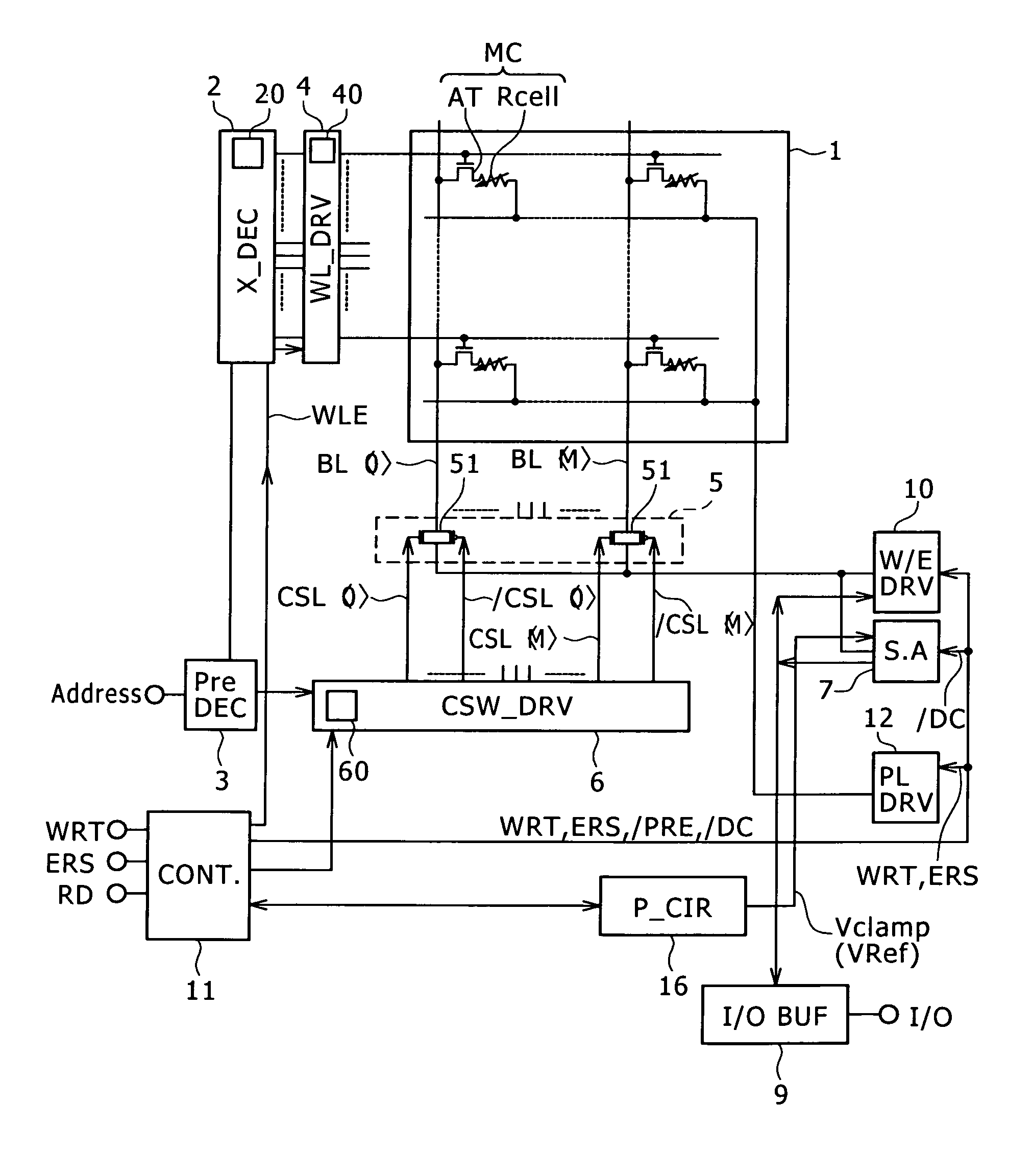
[Memory Cell Configuration]

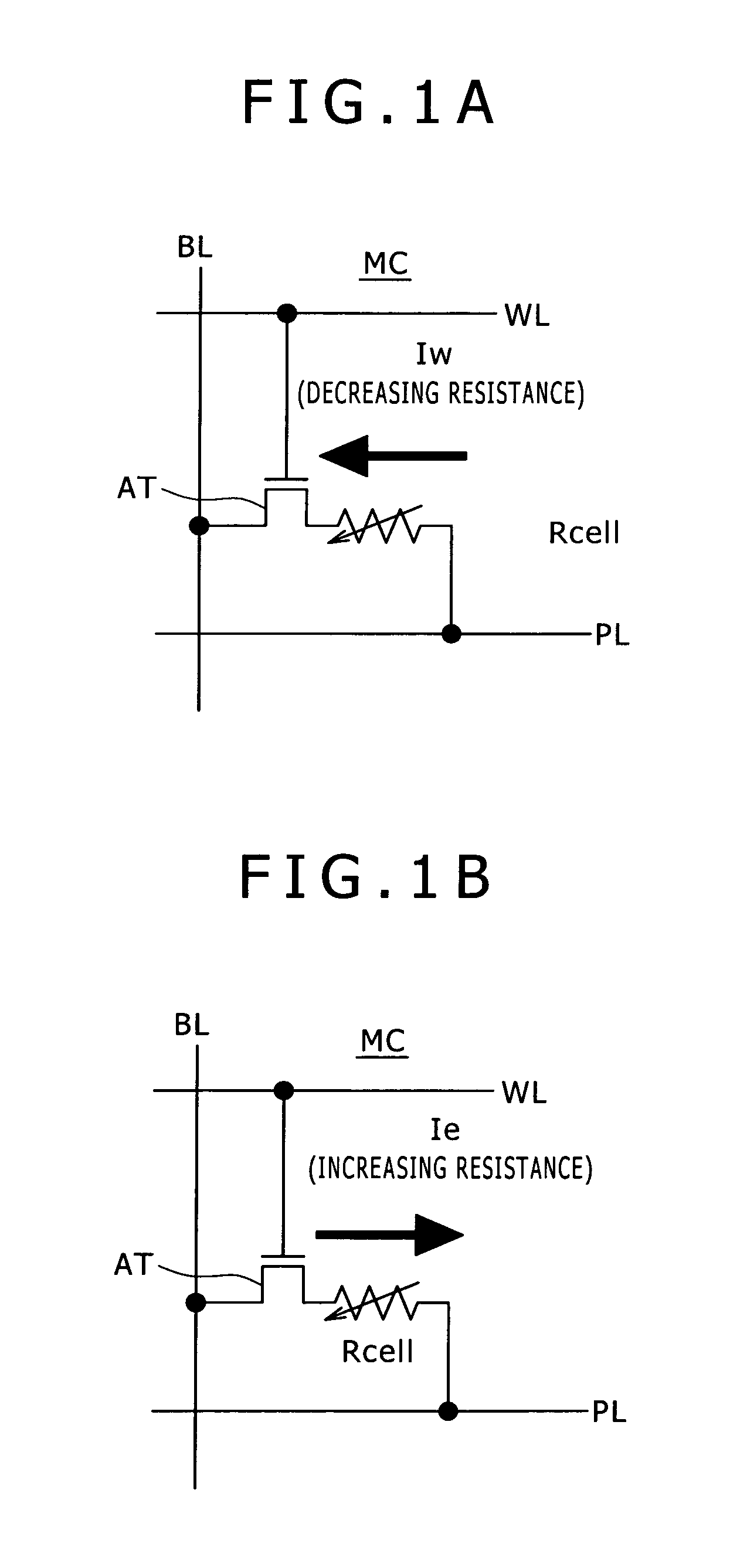
[0072]FIG. 1A and FIG. 1B are diagrams of an equivalent circuit of a memory cell common to embodiments of the present invention. Incidentally, while FIG. 1A shows the direction of a writing current Iw, and FIG. 1B shows the direction of an erasing current Ie, the configuration of the memory cell itself is common to both diagrams.

[0073]The memory cell MC illustrated in FIGS. 1A and 1B has one memory cell resistance Rcell as the “variable cell resistance Rcell” and one access transistor AT.

[0074]One terminal of the memory cell resistance Rcell is connected to a plate line PL. Another terminal of the memory cell resistance Rcell is connected to the source of the access transistor AT. The drain of the access transistor AT is connected to a bit line BL. The gate of the access transistor AT is connected to a word line WL as an “access line.”

[0075]Incidentally, while the bit line BL and the plate line PL are orthogonal to each other in FIGS. 1A and 1B, the bit li...

second embodiment

[0183]The present embodiment and subsequent embodiments represent modifications of circuit configurations of the sense amplifier and the like. Thus, a general configuration, circuits and block configurations other than those related to the modifications, and the basics of operation are similar to those of the first embodiment. Description will therefore be made centering on the modifications.

[0184]FIG. 14 is a schematic diagram of a column circuit configuration according to the present embodiment. FIGS. 15A to 17C2 show control waveforms and timing of a dynamic read, a static read, and a hybrid read.

[0185]Supplied pulses are determined so as to correspond to reversed conductivity types of main transistors (FIG. 15A, FIG. 15B, FIG. 16A, FIG. 16B, FIG. 17A, and FIG. 17B). In addition, inverted signals (high active signals) of the first load control signal ( / DC) and the precharge signal ( / PRE), which inverted signals are denoted with “ / ” removed, are supplied from a control circuit 11 ...

third embodiment

[0187]FIG. 18 is a schematic diagram of a column circuit configuration according to a third embodiment. FIGS. 19A to 21C2 show control waveforms and timing of a dynamic read, a static read, and a hybrid read.

[0188]The circuit configuration shown in FIG. 18 is different from that of FIG. 9 in that a voltage applied to a plate line PL connected to a variable cell resistance Rcell is a readout BL voltage VR (>0), and in that a voltage line connected to a precharge transistor 71 is conversely a GND voltage supply line. That is, the direction of a cell current is reversed. In addition, the precharge transistor 71 and a first control switch 72 are changed from a PMOS transistor to an NMOS transistor, and a load separating switch 52 is changed from an NMOS transistor to a PMOS transistor. The orientation of a current source connected to the first control switch 72 (direction of a current made to flow) is also reversed.

[0189]The other configuration on a memory cell side in FIG. 18 is simila...


PUM


Abstract

A nonvolatile semiconductor memory device includes: a memory element in which a rate of charge discharge between two electrodes of the memory element differs according to a logical value of stored information; cell wiring connected to one electrode of the memory element; a sense amplifier having a sense node connected to the cell wiring, the sense amplifier reading the logical value of the information by comparing a potential of the sense node with a reference potential; and a readout control circuit capable of switching between a dynamic sense operation performing readout by precharging the cell wiring and discharging or charging the cell wiring via the memory element and a static sense operation performing readout in a state of a current load being connected to the sense node.

Description

BACKGROUND OF THE INVENTION[0001]1. Field of the Invention[0002]The present invention relates to a nonvolatile semiconductor memory device having a variable cell resistance Rcell in which a rate of charge discharge between two electrodes of the variable cell resistance Rcell differs according to the logical value of stored information.[0003]2. Description of the Related Art[0004]A nonvolatile memory device in which a precharge voltage is applied to a bit line, and a difference in rate of discharge of the precharge voltage is read out is known.[0005]A nonvolatile semiconductor memory device to which such a readout method can be applied is typified by a (flash) EEPRPM.[0006]Meanwhile, a resistance change type memory device is drawing attention as a nonvolatile memory device in which data is rewritable at high speed, to replace an FG type (flash) EEPROM.[0007]As a resistance change type memory device, a so-called ReRAM is known in which a resistance change when conductive ions are inpu...

Claims


Application Information

Patent Timeline
Patent Type & Authority Patents(United States)
IPC IPC(8): G11C11/00
CPCG11C7/1048G11C7/12G11C13/0004G11C13/004G11C13/0061G11C13/0007G11C2013/0054G11C13/00G11C16/26
Inventor KITAGAWA, MAKOTOSHIIMOTO, TSUNENORITSUSHIMA, TOMOHITO
Owner SONY CORP
Why Eureka
Try Eureka