High throughput, low cost dual-mode patterning method for large area substrates

a dual-mode patterning and large-area substrate technology, applied in the field of high throughput, low cost dual-mode patterning method for large-area substrates, can solve the problems of affecting the commercial implementation of contact printing methods for applications requiring high-resolution patterning, affecting the pattern fidelity and resolution of the patterning achieved using this photolithographic technique, and affecting the quality of the finished product. , to achieve the effect of reducing the complexity of costly and time-consuming photolithographi

Active Publication Date: 2013-04-16
THE BOARD OF TRUSTEES OF THE UNIV OF ILLINOIS +1
View PDF75 Cites 15 Cited by
  • Summary
  • Abstract
  • Description
  • Claims
  • Application Information

AI Technical Summary

Benefits of technology

[0015]This invention provides processing steps, methods and materials strategies for making patterns of structures for electronic, optical and optoelectronic devices. Methods of the present invention are complementary to conventional microfabrication and nanofabrication platforms, and can be effective integrated into existing photolithographic, etching and thin film deposition patterning strategies, systems and infrastructure. Methods of the present invention provide versatile fabrication pathways for making a range of useful structures and devices that eliminate complex, costly and time consuming photolithographic patterning and photoresist development processing steps.
[0016]Methods of the present invention provide a high-throughput, low cost, patterning platform that is an alternative to conventional photolithography and direct laser ablation patterning techniques. The present processing methods are useful for making patterns of microsized and / or nanosized structures having accurately selected physical dimensions and spatial orientation that comprise active and passive components microelectronic devices. Processing provided by the present methods is compatible with large area substrates, such as device substrates for semiconductor integrated circuits, displays, and microelectronic device arrays and systems, and is useful for fabrication applications requiring patterning of layered materials, such as patterning thin film layers in thin film electronic devices. The present methods are compatible with a range of patterned materials, including inorganic and organic semiconductors, conductors, optical functional materials (e.g., light emitting materials) and dielectrics, and are capable of making patterns of structures with high resolution, good pattern fidelity and high precision. In specific embodiments, methods of the present invention enable important processing steps and low cost fabrication strategies for patterning optically transparent layers, such as indium tin oxide layers or doped zinc oxide layers, on devices substrates prepatterned with device components, for example in the fabrication of large area display panel devices, such as TFT-LCDs, OLEDs and PDPs.

Problems solved by technology

There are significant disadvantages associated with this mask configuration, however, which impede commercial implementation of contact printing methods for applications requiring high resolution patterning.
First, mechanical contact between mask and PR can introduce unwanted changes in the optical transmission properties of the mask, thereby undermining the pattern fidelity and resolution of the patterning achieved using this photolithographic technique.
For example, mechanical contact between the PR layer may introduce optical defects and distortions capable of decreasing transmission of the illumination in specific portions of the mask, thereby resulting in pattern defects.
Second, repeated mechanical contact between mask and PR layer results in mask degradation over time, thereby introducing pattern defects and limiting effective mask lifetime.
Given the disadvantages inherent to contact printing systems, projection imaging methods are more commonly used photolithographic patterning techniques for fabrication of integrated circuits, displays and other microelectronic products.
A disadvantage of scan-type projection methods, however, is the significant price of scan-type projection systems capable of large area patterning.
For example, the price of critical optical components, such as lenses, can become prohibitively for large area scan-type projection systems, thus placing practical limitations on commercial implementation of this technique for some important applications.
The multi-step nature of processing in stepping-type projection methods, however, decreases total throughput and makes this technique susceptible to processing errors related to the alignment and registration of independently processed substrate segments. FIG. 1 provides a schematic diagram illustrating mechanical alignment and registration problems which can arise in stepping-type projection photolithography methods.
In the case of fabrication TFT-LCD display devices, this non-uniform pattern in the substrate, as also known as a stitching problem, can result in unwanted non-uniform images.
Total fabrication times provided by laser ablation systems are also low due the direct nature of this patterning technique.
Implementation of direct laser ablation methods for making large area microelectronic applications, is currently restricted, however, due to significant limitations in the classes of materials that can be effectively patterned via laser ablation.
Despite the demonstrated capability of direct patterning of ITO films via laser ablation, these methods are susceptible to drawbacks which significantly hinder its commercial implementation in various device fabrication applications.
First, patterning via direct ablation may result in the build up of ITO ablation debris on the substrate surface that can cause electrical shorts between patterned ITO features.
Such ablation debris caused shorts can negatively affect device performance, for example, by causing a point or line defect in a microelectronic display device.
Second, direct laser ablation of thin ITO films can result in unwanted exposure of the substrate to significant radiant energies of laser electromagnetic radiation.
For application requiring ITO patterning on substrates prepatterned with electronic device components, such as thin film transistor components of microelectronic display devices, this exposure can result in unwanted changes in the electronic, optical and / or mechanical properties of device components underlying the patterned ITO layer.
These changes can result in significant degradation of overall device capabilities and performance.
Third, it is not clear that direct ablation methods are capable of providing the pattern linearity necessary for some device fabrication applications, such as In-Plane Switch (IPS) mode TFT-LCD systems, requiring very high resolution patterning of ITO components.

Method used


Image

  • High throughput, low cost dual-mode patterning method for large area substrates
  • High throughput, low cost dual-mode patterning method for large area substrates
  • High throughput, low cost dual-mode patterning method for large area substrates

Examples


example 1

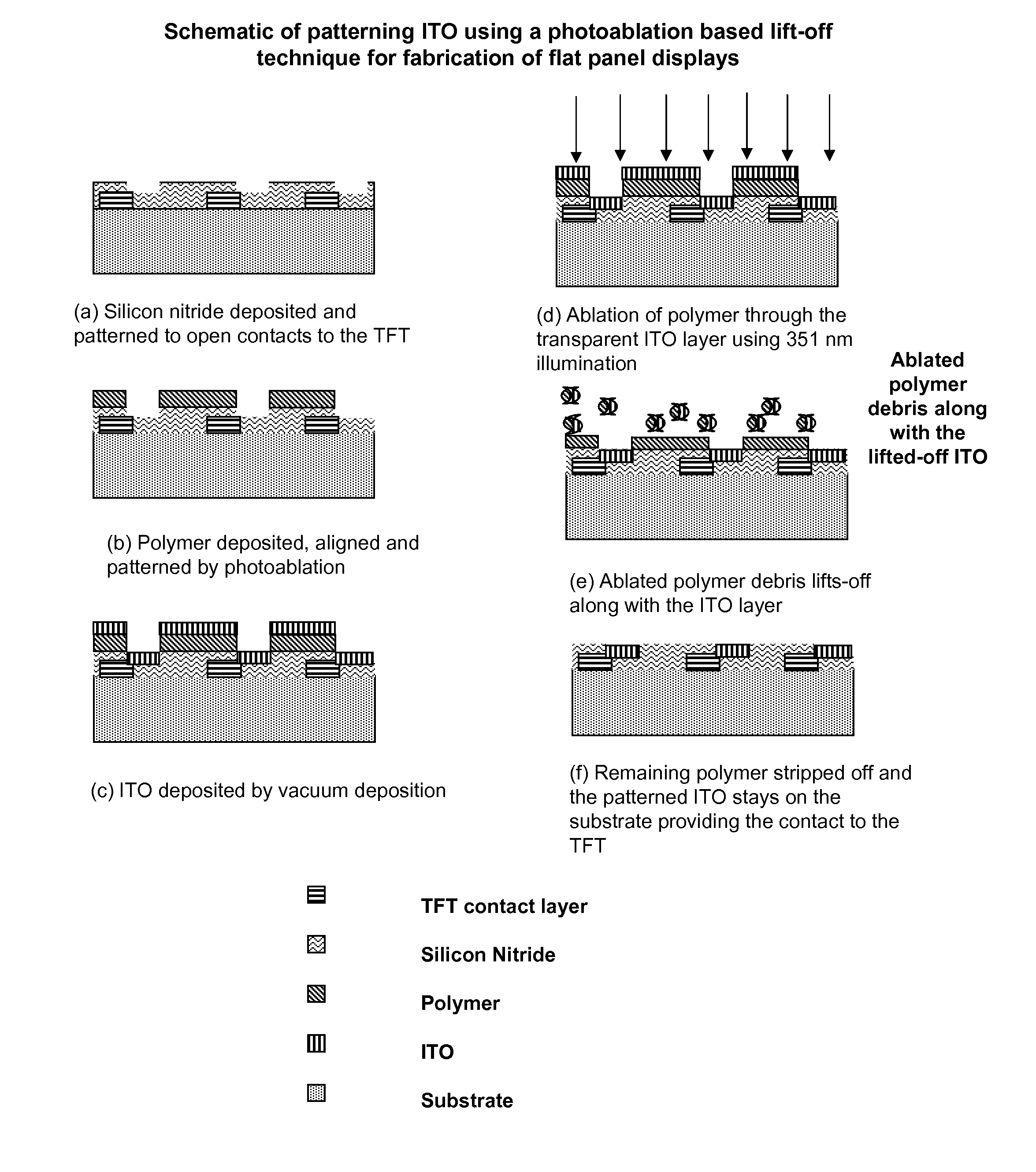
ITO Thin Film Patterning for The Fabrication Of Thin Film Transistor-Liquid Crystal Display Systems

[0084]It is a goal of the present invention to provide a high throughput and low cost patterning platform for making large area microelectronic display devices. The present example provides processing steps and materials strategies for making an important class of flat panel display devices comprising thin film transistor—liquid crystal display systems.

1.a. Basic Principle of Flat Panel Display Devices

[0085]The images in flat panel displays (FPD) are composed of millions or more, colored dots controlled by outer devices. These dots are called pixels and each pixel is the basic unit for image generation. The pixels in the FPD emit controlled-colored-light to the designated directions. A pixel can make various colors by generating light by itself, or by controlling the amount of light that is generated by the attached light source. For generating images in FPD, each pixel should be contr...

example 2

Fabrication of AlNd Pattern in TFT-LCD Panel

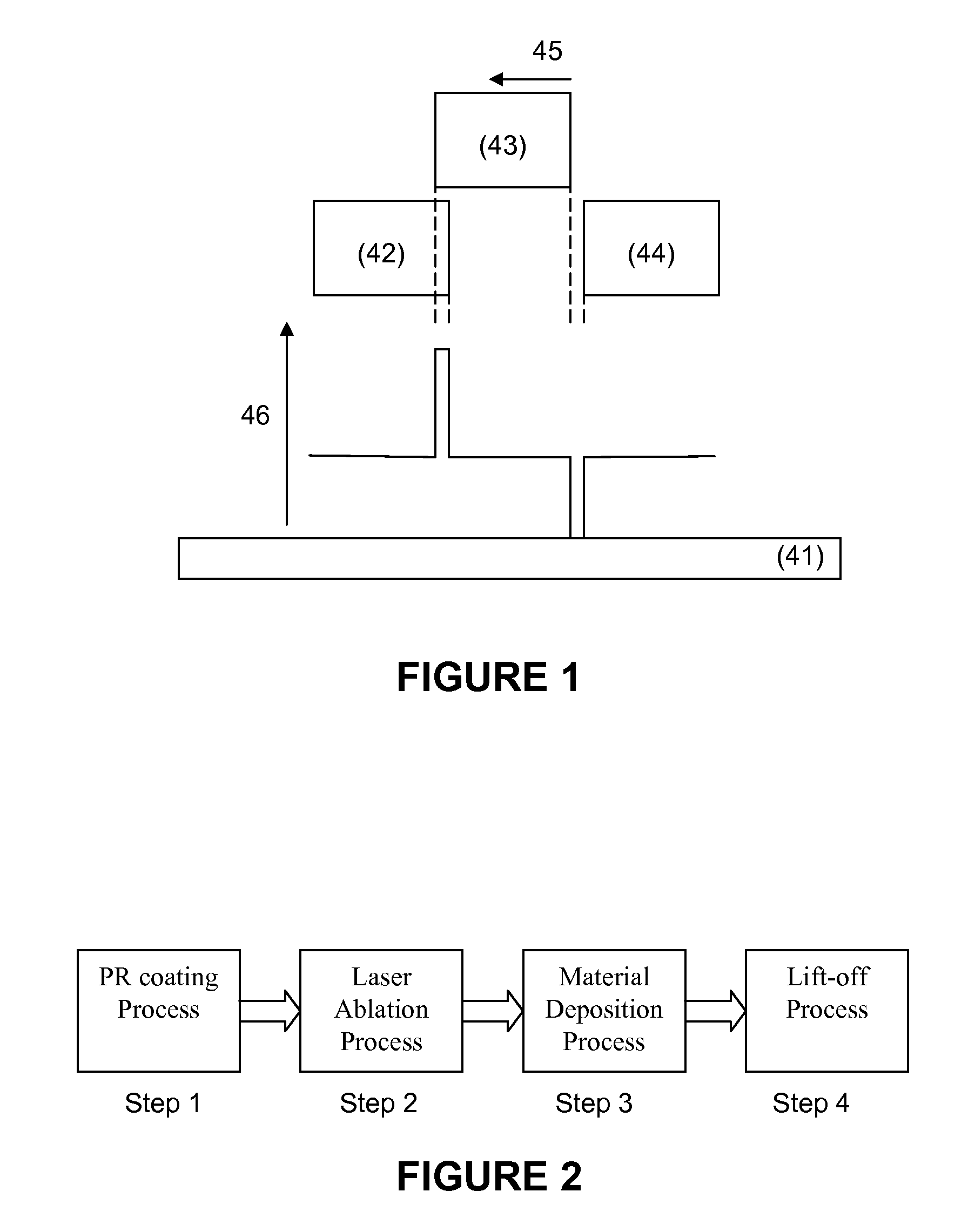
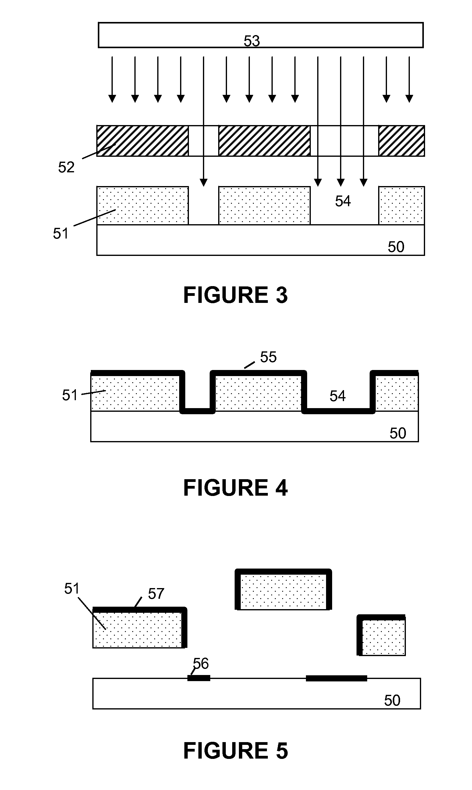
[0104]As is shown in FIG. 16, the gate metal 70 is deposited on the glass substrate 76 to fabricate TFT structures. AlNd (Nd<5%) is commonly used material for this purpose. The conventional pattering method for AlNd is photolithography and wet etching method. The laser ablation of AlNd is known to be very hard due to material characteristics. However, the present invention can be applied to patterning of AlNd layer to achieve cost effective and high resolution patterning. In these methods, patterned laser ablation of a deposited polymer is used to generate a deposition mask, similar to the processing described in the context of ITO patterning. The present methods do not require direct laser ablation patterning of AlNd. As will be apparent to one of ordinary skill in the art, other materials can be patterned by the present methods, thereby eliminating the need for conventional photolithography and etching processing steps.


PUM

PropertyMeasurementUnit
distanceaaaaaaaaaa
thicknessesaaaaaaaaaa
wavelengthsaaaaaaaaaa

Abstract

A high-throughput, low cost, patterning platform is provided that is an alternative to conventional photolithography and direct laser ablation patterning techniques. The processing methods are useful for making patterns of microsized and / or nanosized structures having accurately selected physical dimensions and spatial orientation that comprise active and passive components of a range of microelectronic devices. Processing provided by the methods is compatible with large area substrates, such as device substrates for semiconductor integrated circuits, displays, and microelectronic device arrays and systems, and is useful for fabrication applications requiring patterning of layered materials, such as patterning thin film layers in thin film electronic devices.

Description

CROSS-REFERENCE TO RELATED APPLICATIONS[0001]Not applicable.STATEMENT REGARDING FEDERALLY SPONSORED RESEARCH OR DEVELOPMENT[0002]Not applicable.BACKGROUND OF INVENTION[0003]Microfabrication and nanofabrication processing provide commercially attractive techniques for patterning structures comprising active and passive components of electronic, optical and optoelectronic devices and device arrays. The spectrum of available techniques include photolithography, soft lithography (e.g., contact printing), electron beam direct writing, and photoablation patterning methods. These techniques provide fabrication pathways for making, assembling and integrating large numbers of nanosized and or microsized structures comprising a variety of useful functional materials. Available techniques also provide a high degree of deterministic control over the physical dimensions and spatial arrangement of patterned structures and are compatible with processing a range of substrate materials, morphologies...

Claims


Application Information

Patent Timeline
Patent Type & Authority Patents(United States)
IPC IPC(8): B23K26/16G21H5/00H01L21/44B29C35/08
CPCH01L21/0272H01L27/1288H01L27/124H01L21/0275
Inventor JAIN, KANTICHAE, JUNGHUNAPPASAMY, SREERAM
Owner THE BOARD OF TRUSTEES OF THE UNIV OF ILLINOIS
Why Eureka
Try Eureka