Thermal fluid flow sensor having stacked insulating films above and below heater and temperature-measuring resistive elements

a technology of thermal fluid flow sensor and insulating film, which is applied in the direction of ohmic resistance heating, liquid/fluent solid measurement, instruments, etc., can solve the problem of the insulating film is designed to be a flat film, and the wiring shape is not considered in the above-mentioned techniques, etc. problem, to achieve the effect of eliminating the deflection of the diaphragm, reducing unevenness and large variation

Active Publication Date: 2013-04-30
HITACHI ASTEMO LTD
View PDF27 Cites 9 Cited by
  • Summary
  • Abstract
  • Description
  • Claims
  • Application Information

AI Technical Summary

Benefits of technology

[0009]While there are a planarizing processing using the spin on glass for reducing unevenness on the wiring and a planarizing technique of insulating films by the CMP method, as the wiring pattern on the diaphragm has a large variation in roughness and denseness, the total film thickness of the insulating film in the diaphragm has a large difference between a portion without the wirings and the heater portion and the sensor portion of the microprocessed wirings, resulting in a deflection due to an imbalance of stress.
[0010]A preferred aim of the present invention is to eliminate the deflection of the diaphragm due to an imbalance of stress even when microprocessing of wirings is performed and to provide a thermal fluid flow sensor having a high detection accuracy in a flow measurement.
[0016]When a film having tensile stress equivalent to tensile stress of an upper layer of the sensor is added to a lower layer of the sensor, the tensile stress can be larger than remnant stress of a setting value of the heater, and thus deflection in the diaphragm including the sensor portion underwent a microprocessing is prevented so that a thermal fluid flow sensor having a high accuracy and small resistance fluctuation is provided.

Problems solved by technology

The above-mentioned techniques, however, do not consider an influence from the wiring shape due to processings.
When wirings of the sensor portion are subjected to microprocessing to obtain a high resistance value as required for an improvement in sensitivity, the pitch of the line width and line spacing is narrowed, and thus the coverage of the insulating film to be formed on the wirings are damaged, causing a shift in a remnant stress value of the insulating film which is designed to be a flat film.
Particularly, as to a film having tensile stress, since a silicon nitride film having very large remnant stress per unit film thickness is used, an influence of unevenness becomes large when the film is formed thinner, resulting in a change of the remnant stress of the wiring portion underwent microprocessing to compressive stress, and thus a deflection occurs in the film due to an imbalance of stress in the diaphragm to change the resistance values of the heater and sensor.
Thereby, when the diaphragm is operated as being set by a setting value while the resistance value is being changed, problems such as a lowering in detection accuracy due to a lowering in ΔTh, a destruction of the film structure due to abnormal heating of the heater by an excess current, and so forth occur.
While there are a planarizing processing using the spin on glass for reducing unevenness on the wiring and a planarizing technique of insulating films by the CMP method, as the wiring pattern on the diaphragm has a large variation in roughness and denseness, the total film thickness of the insulating film in the diaphragm has a large difference between a portion without the wirings and the heater portion and the sensor portion of the microprocessed wirings, resulting in a deflection due to an imbalance of stress.

Method used


Image

  • Thermal fluid flow sensor having stacked insulating films above and below heater and temperature-measuring resistive elements
  • Thermal fluid flow sensor having stacked insulating films above and below heater and temperature-measuring resistive elements
  • Thermal fluid flow sensor having stacked insulating films above and below heater and temperature-measuring resistive elements

Examples


first embodiment

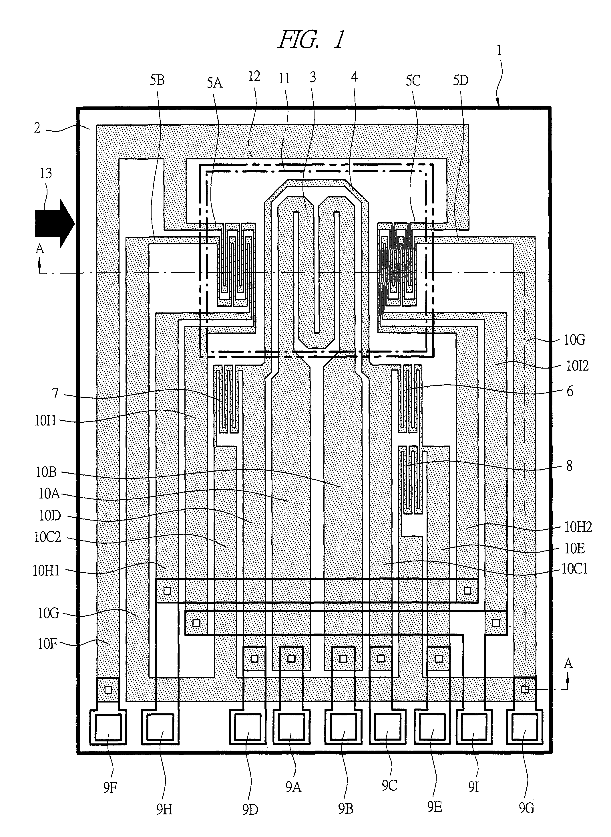
[0041]A plan view of main parts of an example of a thermal fluid flow sensor according to a first embodiment is illustrated in FIG. 1.

[0042]A measuring element 1 which is the thermal fluid flow sensor of the first embodiment is composed of a semiconductor substrate 2, a heater resistive element 3, a temperature-measuring resistive element for heater resistive element 4, a temperature-measuring resistive element, an air-temperature-measuring resistive element 6, heater-temperature-controlling resistive elements 7 and 8, terminal electrodes 9A to 9I, and draw-out wirings 10A, 10B, 10C1, 10C2, 10D, 10E, 10F, 10G, 10H1, 10H2, 10I1, and 10I2, etc.

[0043]The semiconductor substrate 2 is formed of, for example, single crystal silicon (Si).

[0044]The heater resistive element 3 is formed on the semiconductor substrate 2 interposing an insulating film, and has a wiring width of, for example, about 1 to 150 μm.

[0045]The temperature-measuring resistive element for heater resistive element 4 is us...

second embodiment

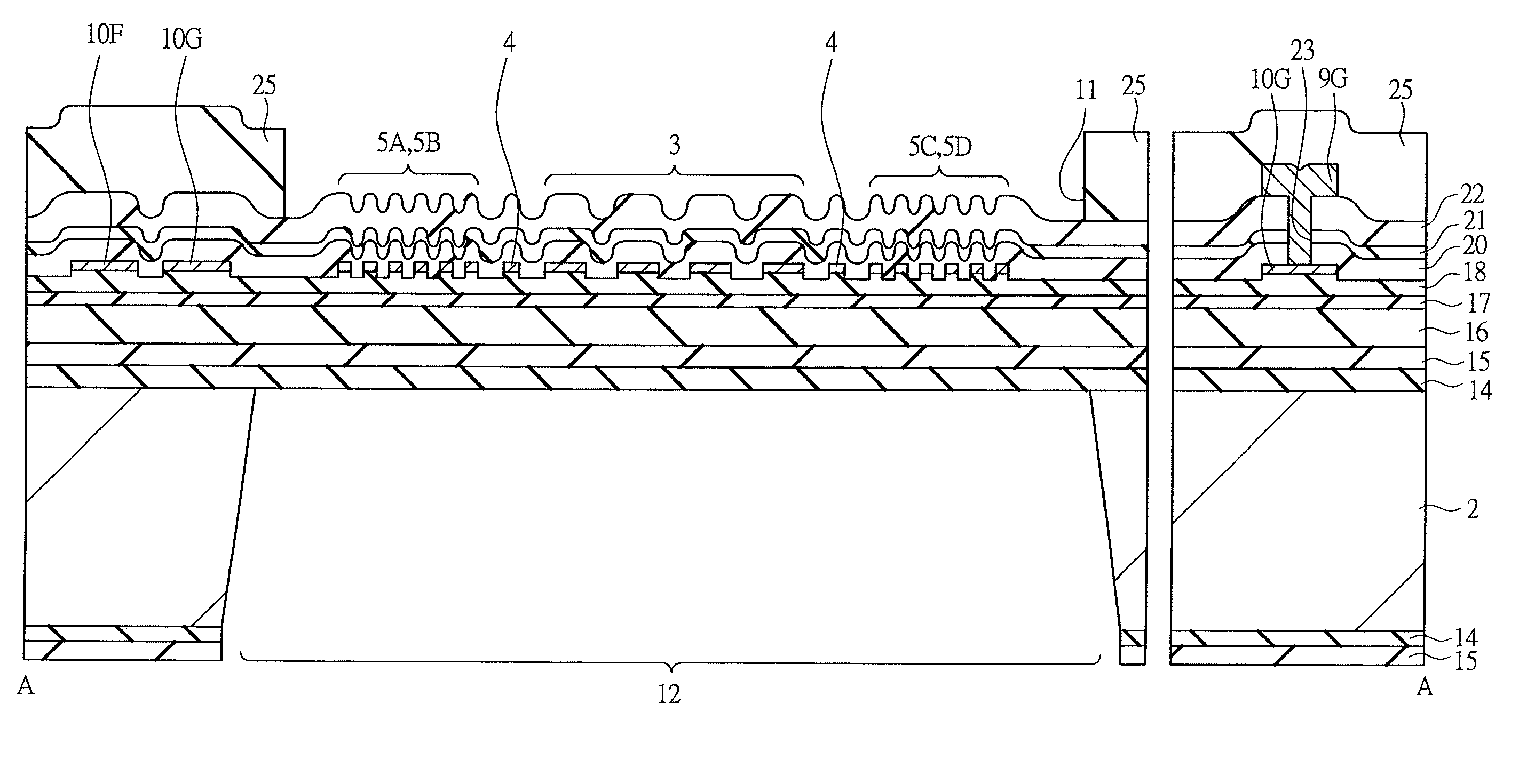
[0097]In a second embodiment, prevention of warpage of a wafer due to remnant stress which a film deposited on the wafer (the semiconductor substrate 2) has is considered.

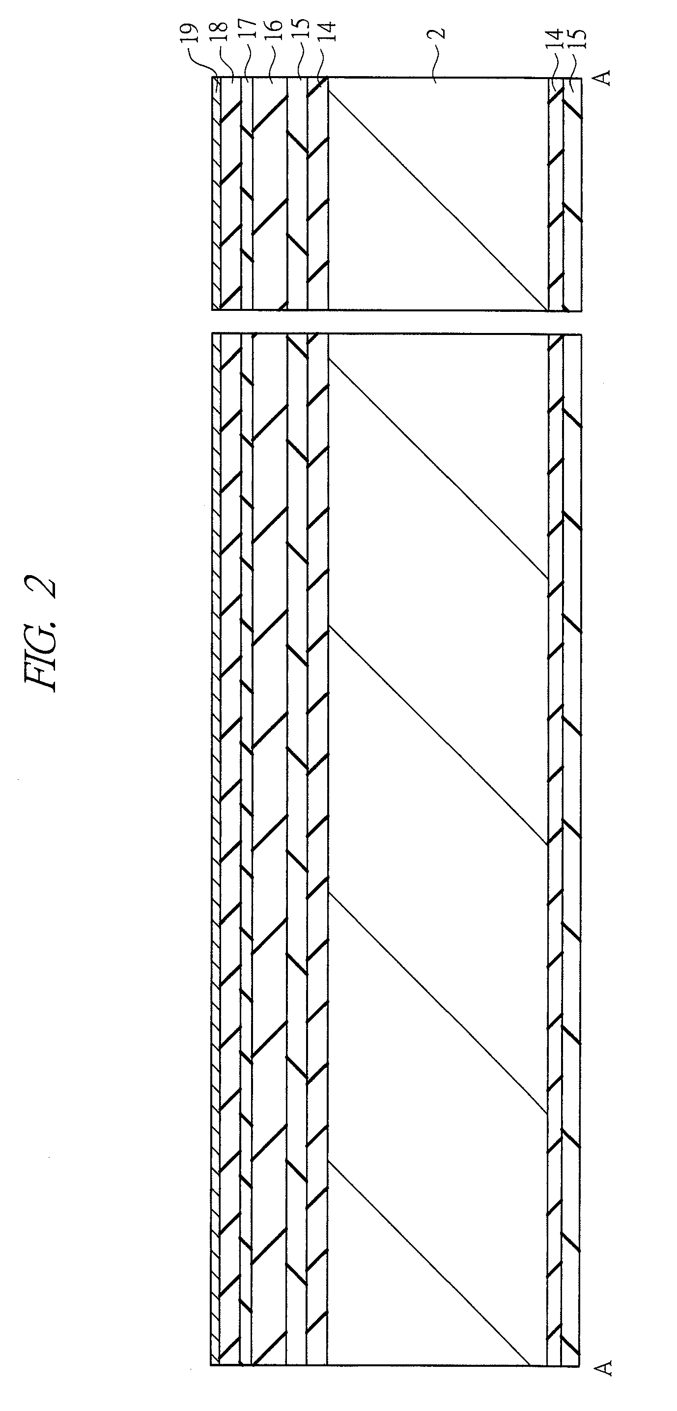
[0098]FIG. 16 illustrates an example of a thermal fluid flow sensor according to the second embodiment, illustrating a cross-sectional view of main parts taken along the line A-A in FIG. 1 of the first embodiment.

[0099]Thicknesses of respective films configuring the thermal fluid flow sensor of the second embodiment are the same with those of the first embodiment except for the fourth insulating film 17 (a silicon nitride film) having a thickness of about 200 nm (it has been about 140 nm in the first embodiment).

[0100]Next, a manufacturing process of the thermal fluid flow sensor according to the second embodiment will be described. Note that the manufacturing process of the thermal fluid flow sensor of the second embodiment is the same with that of the first embodiment until the step of depositing the fourth insul...


PUM

PropertyMeasurementUnit
tensile stressaaaaaaaaaa
compressive stressaaaaaaaaaa
thicknessaaaaaaaaaa

Abstract

A thermal fluid flow sensor having a diaphragm structure body configured by an insulating film formed by stacking a film having compressive stress and a film having tensile stress on the top and bottom of a temperature-measuring resistive element and a heater resistive element which are processed by microprocessing is provided. The insulating film at a lower layer of the heater resistive element, a temperature-measuring resistive element for heater resistive element, upstream temperature-measuring resistive elements, and downstream temperature-measuring resistive elements, has films having compressive stress (a first insulating film, a third insulating film, and a fifth insulating film) and films having tensile stress (a second insulating film and a fourth insulating film) being alternately arranged, and two layers or more of the films having tensile stress are arranged.

Description

CROSS-REFERENCE TO RELATED APPLICATION[0001]The present application claims priority from Japanese Patent Application No. JP 2008-312359 filed on Dec. 8, 2008, the content of which is hereby incorporated by reference into this application.TECHNICAL FIELD OF THE INVENTION[0002]The present invention relates to a thermal fluid flow sensor and a manufacturing technique of the thermal fluid flow sensor. More particularly, the present invention relates to a technique effectively applied to a thermal fluid flow sensor suitable for a thermal fluid flow meter which measures intake air of an internal-combustion engine.BACKGROUND OF THE INVENTION[0003]Among fluid flow sensors which are used in an air flow meter for measuring an intake air amount provided to an electronically-controlled fuel injection device for an internal-combustion engine in, e.g., vehicles, thermal fluid flow sensors are in the main stream because they can directly detect a mass amount of air.[0004]Among those thermal fluid ...

Claims


Application Information

Patent Timeline
Patent Type & Authority Patents(United States)
IPC IPC(8): G01F1/68
CPCB81B3/0072G01F1/692G01F1/699G01F5/00G01F1/6845B81B2201/0292B81B2203/0127Y10T29/49083
Inventor SAKUMA, NORIYUKI
Owner HITACHI ASTEMO LTD
Why Eureka
Try Eureka