Method of fabricating an epitaxial layer

a technology of epitaxial layer and layer layer, which is applied in the direction of basic electric elements, electrical apparatus, and semiconductor devices, etc., can solve the problems of unstable electrical performance of mos transistors and difficult control

Active Publication Date: 2013-05-21
UNITED MICROELECTRONICS CORP
View PDF141 Cites 0 Cited by
  • Summary
  • Abstract
  • Description
  • Claims
  • Application Information

AI Technical Summary

Benefits of technology

[0009]According to the above, the present invention provides a method of fabricating an epitaxial layer including performing a surface treatment on a recess to form a Si—OH containing surface. An in-situ epitaxial process is performed to form an epitaxial layer within the recess, wherein the in-situ epitaxial process is performed in a hydrogen-free atmosphere and at a temperature lower than 800° C. Therefore, the interface between the epitaxial layer formed by said method and the substrate has a square shape, thereby solving the problem of the interface passivation between the epitaxial layer and the substrate.

Problems solved by technology

However, it's hard to control the level of rounding shape which causes the instability of electrical performance of MOS transistor 100.

Method used


Image

  • Method of fabricating an epitaxial layer
  • Method of fabricating an epitaxial layer
  • Method of fabricating an epitaxial layer

Examples


Embodiment Construction

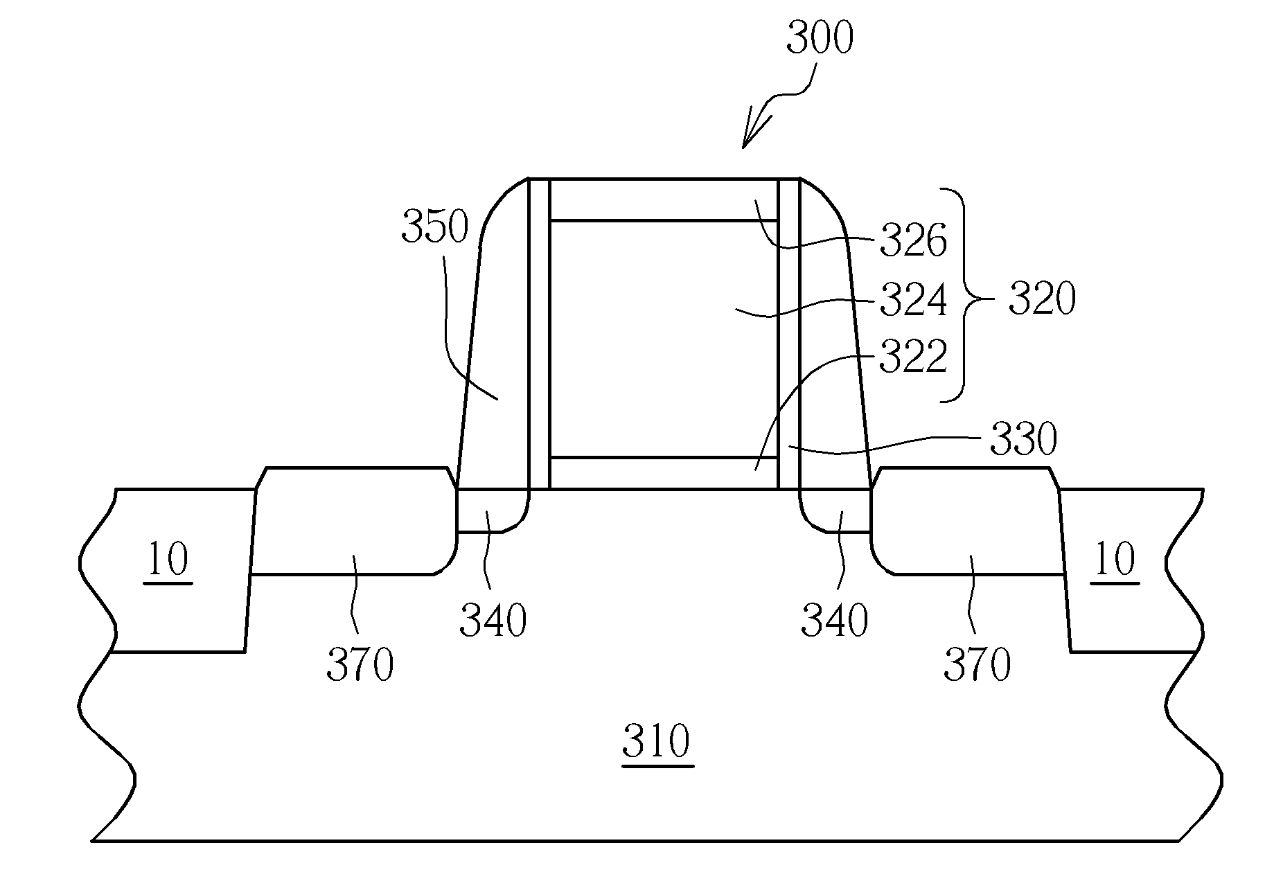
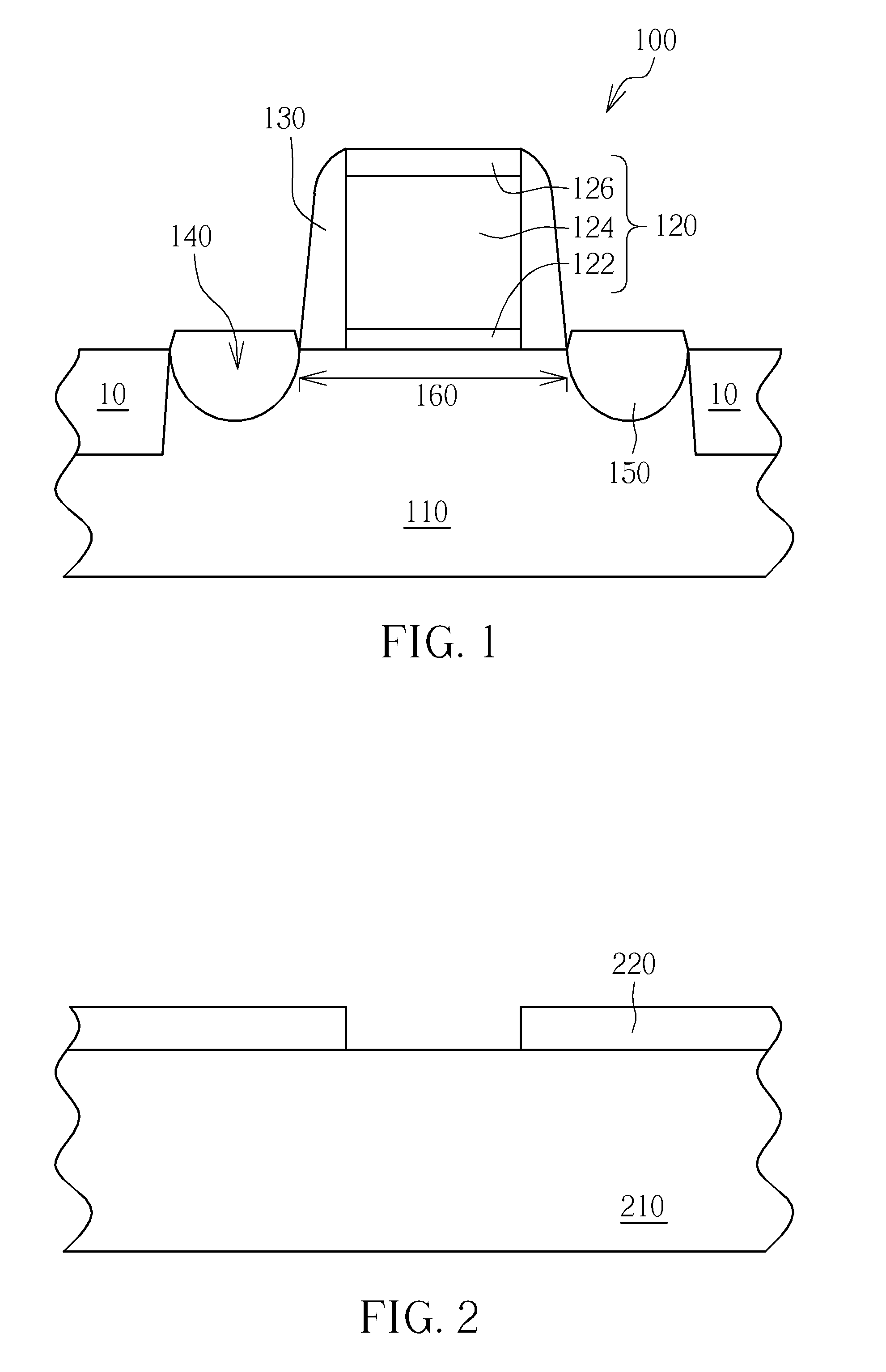
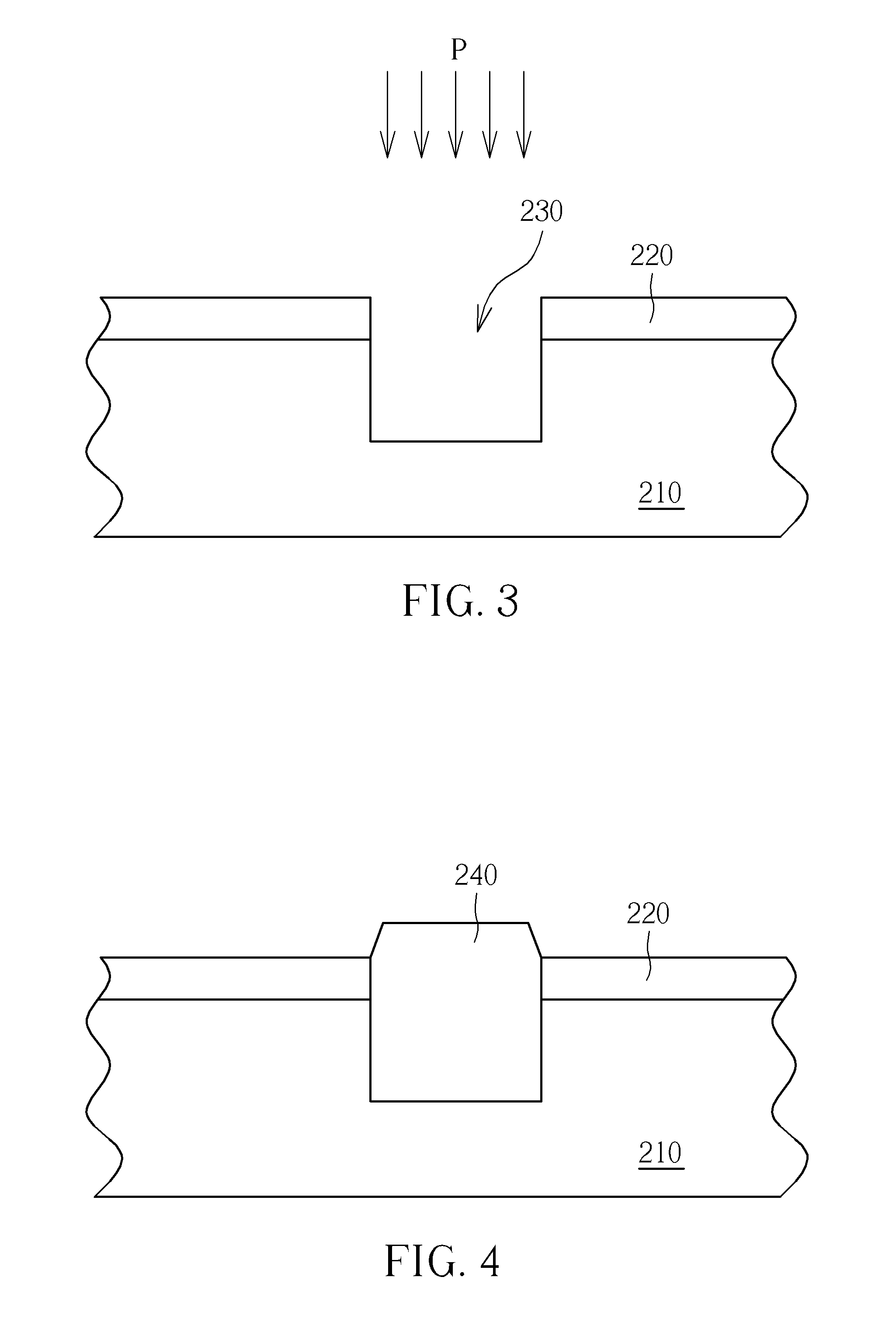
[0016]FIGS. 2-4 schematically depicts a method of fabricating an epitaxial layer according to one preferred embodiment of the present invention. Refer to FIGS. 2-4, a substrate 210 is provided, wherein the substrate 210 includes a semiconductor substrate such as a silicon substrate, a silicon containing substrate, or a silicon-on-insulator (SOI) substrate. A patterned mask 220 is formed on the substrate 210 (As shown in FIG. 2). In this embodiment, the mask 220 may be a silicon nitride layer, and more specifically may be a silicon nitride layer formed by a precursor of hexachlorodisilane (HCD). The mask 220 may be patterned by methods such as etching lithography method, but it is not limited thereto. In another embodiment, the mask 220 may be also made of other materials, and the mask 220 may be formed by a precursor of chlorine containing material or formed by chlorine containing materials, thereby forming the surface of the substrate 210 being attached with chlorine and a chlorine...


PUM

PropertyMeasurementUnit
temperatureaaaaaaaaaa
lattice constantaaaaaaaaaa
band structureaaaaaaaaaa

Abstract

A method of fabricating an epitaxial layer includes providing a substrate. The substrate is etched to form at least a recess within the substrate. A surface treatment is performed on the recess to form a Si—OH containing surface. An in-situ epitaxial process is performed to form an epitaxial layer within the recess, wherein the epitaxial process is performed in a hydrogen-free atmosphere and at a temperature lower than 800° C.

Description

BACKGROUND OF THE INVENTION[0001]1. Field of the Invention[0002]The present invention relates generally to a method of fabricating an epitaxial layer, and more specifically, to a method of fabricating an epitaxial layer performed in a hydrogen-free atmosphere and at a temperature lower than 800° C. thereby making the interface between the epitaxial layer and the substrate have a square shape.[0003]2. Description of the Prior Art[0004]As known in the art, strained silicon technologies have been introduced in the MOS manufacturing process in order to increase the mobility of electrons or holes, thereby attaining higher performance of a semiconductor device. For example, taking advantage of the lattice constant of a SiGe layer being different from that of Si, a strain occurs in the silicon layer growing on the SiGe layer. Since SiGe has a larger lattice constant than Si, the band structure of Si is altered, thereby increasing the mobility of the carriers.[0005]FIG. 1 schematically depi...

Claims


Application Information

Patent Timeline
Patent Type & Authority Patents(United States)
IPC IPC(8): H01L21/20
CPCH01L21/0243H01L21/02529H01L21/02532H01L21/02639H01L21/02658H01L29/66636H01L29/7834H01L29/165
Inventor LU, TSUO-WENLAI, I-MINGHOU, TSUNG-YULIN, CHIEN-LIANGTENG, WEN-YIWANG, SHAO-WEIWANG, YU-RENCHIEN, CHIN-CHENG
Owner UNITED MICROELECTRONICS CORP
Why Eureka
Try Eureka