Semiconductor package and fabrication method thereof

a semiconductor and packaging technology, applied in the direction of semiconductor devices, semiconductor/solid-state device details, electrical apparatus, etc., can solve the problems of long bonding wires, inability to meet the demands the length of the bonding wire loop cannot be further reduced to meet the needs of lighter, thinner and smaller semiconductor products, so as to enhance the electrical connection quality of the semiconductor package, improve the heat dissipation effect, and improve the effect of electrical connection

Active Publication Date: 2013-06-25
SILICONWARE PRECISION IND CO LTD
View PDF18 Cites 2 Cited by
  • Summary
  • Abstract
  • Description
  • Claims
  • Application Information

AI Technical Summary

Benefits of technology

[0021]According to the present invention, the extension pads of the wiring layer made of copper are exposed from the vias so as for the solder balls to be disposed thereon. Due to improved electrical connection between the copper material and the solder material and an increased heat dissipating effect, the present invention enhances the electrical connecting quality of the semiconductor package.
[0022]Further, the carrier of the present invention is made of an iron alloy or a copper alloy, the cost of which is lower than that of pure copper used in the prior art, thereby reducing material costs.
[0023]Furthermore, to dispose the semiconductor package of the present invention on a circuit board, solder balls can be formed on the extension pads in the vias first and then attached to a solder paste having a thickness of 0.1 mm. As such, even if warpage of the semiconductor package occurs, in that the solder balls can be reliably attached to the solder paste, the present invention effectively avoids the conventional problem of poor electrical connection.

Problems solved by technology

However, due to the thickness of the encapsulant of the QFN package, the height of the QFN package cannot be further reduced to meet the demands for lighter, thinner and smaller semiconductor products.
However, if a highly integrated chip is used, since the electrode pads of the chip are configured at a high density, a higher number of conductive pads are required, thus increasing the distance between the conductive pads and the chip and increasing the length of the wire loops of the bonding wires.
Long bonding wires complicates the wire bonding process.
Further, impacted by molding flow during the molding process, long bonding wires may easily sweep or shift so as to come into contact with each other, thereby easily short circuiting and adversely affecting the electrical connection quality of the semiconductor package.
Furthermore, a long distance between the conductive pads and the semiconductor chip may complicate the wire bonding process and even cause failure of the wiring bonding process.
In addition, long bonding wires increase material costs.
However, the electrical connecting and heat dissipating effects between the Ni / Au material 25 and the solder material are quite poor, which results in a low electrical connection quality for the semiconductor package.
Further, the carrier 20 of copper is quite expensive, thereby resulting in higher material costs.
However, if warpage occurs to the semiconductor package 2, a too thin layer of solder paste prevents the Ni / Au material 25 from being reliably attached thereto, thus resulting in a poor electrical connection of the semiconductor package.

Method used


Image

  • Semiconductor package and fabrication method thereof
  • Semiconductor package and fabrication method thereof
  • Semiconductor package and fabrication method thereof

Examples


Embodiment Construction

[0028]The following illustrative embodiments are provided to illustrate the disclosure of the present invention and its advantages, these and other advantages and effects being apparent to those in the art after reading this specification.

[0029]It should be noted that the drawings are not intended to limit the present invention. Various modification and variations can be made without departing from the spirit of the present invention. Further, terms such as “one”, “above”, etc. are merely for illustrative purposes and should not be construed to limit the scope of the present invention.

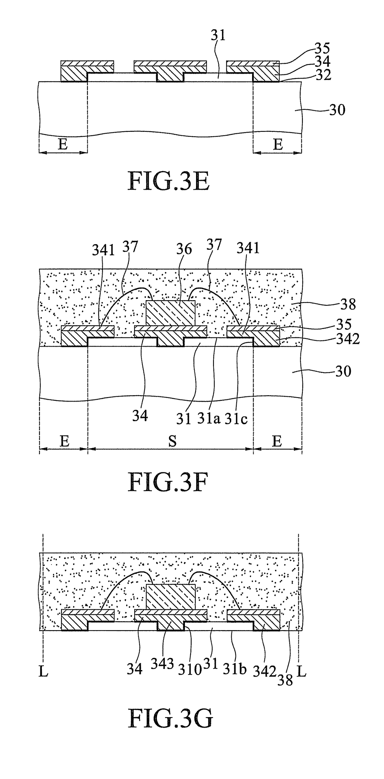
[0030]FIGS. 3A to 3I show a fabrication method of a semiconductor package according to the present invention.

[0031]Referring to FIG. 3A, a carrier 30 made of an iron alloy or a copper alloy is provided, and a carrier region S and an extension region E adjacent to the carrier region S are defined on a surface of the carrier 30.

[0032]Subsequently, a dielectric layer 31 is formed on the carrier region S a...


PUM


Abstract

A semiconductor package includes: a dielectric layer having opposing first and second surfaces and side surfaces; a copper wiring layer disposed on the first surface of the dielectric layer and having extension pads; a surface processing layer disposed on the wiring layer; a semiconductor chip disposed on the wiring layer and electrically connected to the surface processing layer; and an encapsulant disposed on the first surface of the dielectric layer for encapsulating the semiconductor chip, the wiring layer and the surface processing layer while exposing the second surface of the dielectric layer. Further, vias are disposed between the side surfaces of the dielectric layer and the encapsulant such that the extension pads are exposed from the vias so as for solder balls to be disposed thereon. Due to improved electrical connection between the copper and solder materials, the electrical connection quality of the package is improved.

Description

CROSS-REFERENCES TO RELATED APPLICATIONS[0001]This application claims under 35 U.S.C. §119(a) the benefit of Taiwanese Application No. 100121958, filed Jun. 23, 2011, the entire contents of which is incorporated herein by reference.BACKGROUND OF THE INVENTION[0002]1. Field of the Invention[0003]The present invention relates to semiconductor packages, and, more particularly, to a carrier-free semiconductor package.[0004]2. Description of Related Art[0005]Conventionally, there are various kinds of semiconductor packages that use lead frames as chip carriers. For example, a QFN (Quad Flat Non-leaded) semiconductor package is a lead frame-based chip scale package, which is characterized in that the leads thereof do not extend out from the package sides as in a conventional quad flat package (QFP), thereby reducing the size of the semiconductor package.[0006]However, due to the thickness of the encapsulant of the QFN package, the height of the QFN package cannot be further reduced to mee...

Claims


Application Information

Patent Timeline
Patent Type & Authority Patents(United States)
IPC IPC(8): H01L23/52H01L29/40H01L23/48
CPCH01L21/568H01L21/6835H01L23/3128H01L2224/48247H01L2224/48091H01L2924/00014H01L2224/48227H01L24/48H01L2221/68345H01L2224/16245H01L2224/85416H01L2224/85439H01L2224/85444H01L2224/45099H01L24/97H01L2924/181H01L2924/00012
Inventor HUNG, LIANG-YIPAI, YU CHENGSUN, MING CHENLIN, CHUN HSIEN
Owner SILICONWARE PRECISION IND CO LTD
Why Eureka
Try Eureka