
Fabrication technique for high frequency, high power group III nitride electronic devices

a technology of nitride and fabrication technique, which is applied in the direction of basic electric elements, electrical apparatus, semiconductor devices, etc., can solve the problems of increased sub-threshold drain-source leakage current, short channel effect, and low breakdown voltage,

Active Publication Date: 2013-07-02
UNIVERSITY OF SOUTH CAROLINA
View PDF22 Cites 33 Cited by
  • Summary
  • Abstract
  • Description
  • Claims
  • Application Information

AI Technical Summary

Problems solved by technology

However, reducing LG to values where the ratio of LG to the AlGaN barrier thickness is below 20-30, normally results in short-channel effects such as the threshold voltage shift and low breakdown voltages.
This consequence results from the increased sub-threshold drain-source leakage currents.
Apart from the gate to channel separation, the short channel effects and the loss of gate modulation in small gate devices can also result from the poor confinement of the electrons in the two dimensional electron gas (2DEG) channel.
It is now well established that gate leakage currents lead to a power degradation in GaN—AlGaN HFETs.

Method used


Image

  • Fabrication technique for high frequency, high power group III nitride electronic devices
  • Fabrication technique for high frequency, high power group III nitride electronic devices
  • Fabrication technique for high frequency, high power group III nitride electronic devices

Examples


example 1

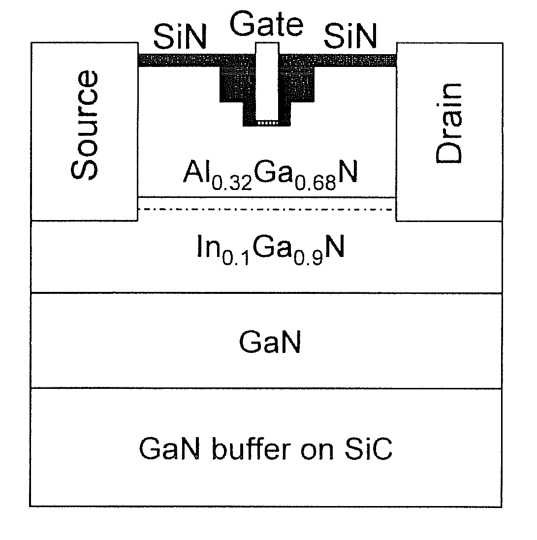
[0080]An AlInGaN / GaN MOS-DHFET sample with an InGaN channel was grown by metalorganic chemical vapor deposition. The material growth procedure was similar to that described in G. Simin, Xuhong Hu, Ahmad Tarakji, Jianping Zhang, Alex Koudymov, Salih Saygi, Jinwei Yang, Asif Khan, Michael S Shur and Remis Gaska, “AlGaN / InGaN / GaN Double Heterostructure Field-Effect Transistor,” Jpn. J. Appl. Phys., Vol 40 (2001), pp L1142-1144. The InGaN layer was grown at 820° C. to assist with the In incorporation. The In composition in the InGaN layer for this structure was calibrated using X-ray diffraction and photoluminescence analysis. A total charge density of around 1.5×1013 cm−2 and a mobility of 1240 cm2 / V-s were obtained by Hall measurements. The AlInGaN barrier had an aluminum alloy composition of 30% which was confirmed by photoluminescence and X-ray measurements. The thickness of the AlGaN barrier was around 200 Å (angstroms).

[0081]Then, the band diagrams of InGaN channel devices and tho...


PUM


Abstract

Fabrication methods of a high frequency (sub-micron gate length) operation of AlInGaN / InGaN / GaN MOS-DHFET, and the HFET device resulting from the fabrication methods, are generally disclosed. The method of forming the HFET device generally includes a novel double-recess etching and a pulsed deposition of an ultra-thin, high-quality silicon dioxide layer as the active gate-insulator. The methods of the present invention can be utilized to form any suitable field effect transistor (FET), and are particular suited for forming high electron mobility transistors (HEMT).

Description

PRIORITY INFORMATION[0001]The present application claims priority to U.S. Provisional Patent Application No. 60 / 875,031 filed on Dec. 15, 2006, naming Asif Khan and Vinod Adivarahan as inventors and U.S. Provisional Application No. 60 / 875,029 filed on Dec. 15, 2006, naming Asif Khan as the inventor, both of which are incorporated herein by reference.GOVERNMENT SUPPORT CLAUSE[0002]The present invention was developed with funding from the Defense Advanced Research Project Agency under contract no. DAAD19-02-1-0282. The government retains certain rights in the invention.BACKGROUND OF THE INVENTION[0003]AlGaN / GaN heterojunction field effect transistors (HFETs) are now well developed for delivering high output powers in the 2-8 GHz range. The focus of the research effort has now shifted to increasing their operating frequencies. The most efficient and direct way of increasing the operational frequencies is to reduce the gate length (LG). However, reducing LG to values where the ratio of ...

Claims


Application Information

Patent Timeline
Patent Type & Authority Patents(United States)
IPC IPC(8): H01L21/338
CPCH01L21/02057H01L21/0214H01L21/02164H01L21/0217H01L21/02211H01L21/02274H01L21/0228H01L21/30621H01L21/3141H01L21/31608H01L21/3185H01L29/66462H01L29/7783H01L29/2003
Inventor KHAN, M. ASIFADIVARAHAN, VINOD
Owner UNIVERSITY OF SOUTH CAROLINA
Learn More