
Anodic bondable porcelain and composition for the porcelain

a technology of anodic bonding and porcelain, applied in the direction of natural mineral layered products, semiconductor/solid-state device details, transportation and packaging, etc., can solve the problems of reducing the size and profile of packaging, enhancing performance, and limiting the reduction of hole size and pitch, so as to reduce the influence of mems, resist cracking, and increase the transverse strength

Inactive Publication Date: 2013-07-09
NDC CORPORATION
View PDF7 Cites 5 Cited by
  • Summary
  • Abstract
  • Description
  • Claims
  • Application Information

AI Technical Summary

Benefits of technology

The patent describes a new material that can be bonded at a low temperature and has superior strength. It is also resistant to cracking and can be easily handled.

Problems solved by technology

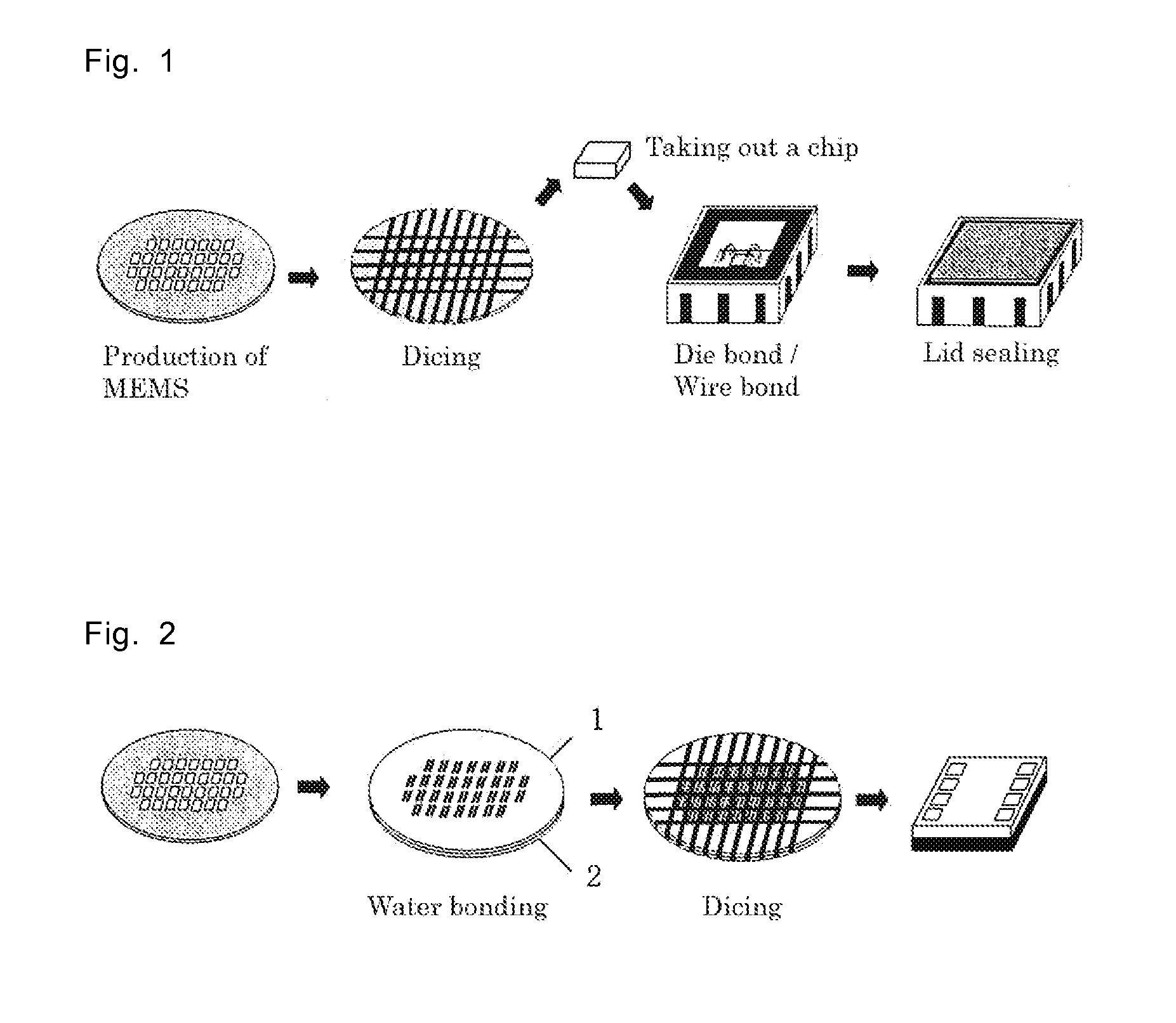
Actually, about 80% of the cost of the MEMS is considered to be charge for mounting using a package and for an inspection, and thus, the package mounting is a serious problem in the reduction in size and profile and the enhancement of performance.
According to the production method by package mounting, there area number of steps as described above, and in addition, the MEMS chip with the moving portion is handled without protection, so the MEMS chip is easily broken, which causes the degradation in yield.
When drilling used for opening a hole in glass is employed, the shape of a hole is satisfactory; however, there is a limit in the reduction in a hole size and a pitch.
Further, when the number of holes in the wafer increases, it becomes difficult to grind the wafer, so there is a limit in the number of holes.
Further, although a number of holes can be concurrently formed by sandblasting, the hole shape is poor and there is also a limit in the hole size and pitch.
After the hole opening, a through wiring treatment is performed, which requires a complicated step.
Thus, sandblasting requires a high cost and is limited in miniaturization.
Silicon can be subjected to fine hole opening using a Deep RIE apparatus; however, the Deep RIE apparatus is very expensive and takes a long treatment time.
However, the bonding apparatus is quite expensive and takes a long bonding time.
Thus, although a substrate having fine holes can be produced, there is a problem in that the considerable capital investment is required, and cost is high.
However, with those materials, the step of forming through wiring is complicated and its cost is high, and furthermore, a multi-layered wiring cannot be formed, so there is no degree of freedom in design.
It is difficult to form a multi-layered wiring with glass or silicon.
However, the thermal expansion coefficient of the LTCC substrate is not matched with that of silicon, and a method of bonding to silicon is limited to a method using an inclusion such as soldering, a wax material, glass or an organic adhesive.
Therefore, it has been difficult to adopt the LTCC substrate in view of the reliability in bonding to a wafer.
Therefore, if the material does not have a thermal expansion coefficient similar to that of silicon, there is a possibility that the electrode position of the MEMS wafer may be displaced from the electrode position of the mounting substrate due to heat stress.
(b) While a prototype was made, it was found that a thin substrate with a large diameter is likely to crack and has an unstable handling property, and a material with high strength is required.

Method used


Image

  • Anodic bondable porcelain and composition for the porcelain
  • Anodic bondable porcelain and composition for the porcelain

Examples


examples

[0088]Hereinafter, the present invention will be described in more detail by way of examples and comparative examples. However, the present invention is not limited thereto.

examples 1 to 9

[0089]Li2CO3, MgO, Al2O3, SiO2 and Bi2O3 with an average particle size of 1 μm or less were mixed so that a content ratio in the oxide conversion became to that as shown in Table 1, and the mixture was calcined at 750 to 850° C. and crushed to obtain powder. An organic binder, a plasticizer and toluene were added to the calcined product to form a green sheet with a thickness of 150 μm by a doctor blade method. Then, five green sheets were laminated, and thermally compressed under a pressure of 150 kg / cm2 at a temperature of 70° C. The thus-obtained laminated body was subjected to binder-removal in the air at 500° C., thereby to obtain a multi-layered substrate made of a porcelain fired in the air under the conditions as in Table 1.

[0090]Nine levels of the substrates densified (water absorption: zero) at a firing temperature of 850 to 900° C. were prepared to evaluate the anodic bonding performance. Each of the nine levels of the substrates was diced to a 20 mm square and mirror-poli...


PUM

PropertyMeasurementUnit
molar ratioaaaaaaaaaa
temperatureaaaaaaaaaa
wt %aaaaaaaaaa

Abstract

An anodic bondable low-temperature fired porcelain having high-strength and low-thermal-expansion, wherein a conductive ion during anodic bonding is an Li ion, containing a complex oxide having a composition represented by the following formula:(1−x)(αLi2O-βMgO-γAl2O3-δSi2O2).xBi2O3  (1)where x represents a mass ratio of 0.01 to 0.1, and α, β, γ and δ have a molar ratio of 2 to 5:1 to 2:1 to 2:7 to 17.

Description

FIELD OF THE INVENTION[0001]The present invention relates to an anodic bondable low-temperature fired porcelain having high-strength and low-thermal-expansion and a composition for the porcelain. More specifically, the present invention relates to a wiring substrate formed by molding and firing the composition, preferably, a fired substrate suitable as a hermetically sealed through wiring substrate of micro electro mechanical systems (MEMS), and an MEMS element formed by wafer-level packaging using the hermetically sealed through wiring substrate.BACKGROUND OF THE INVENTION[0002]Anodic bonding is a method of bonding glass to silicon by bringing glass containing alkali metal typified by borosilicate glass into contact with silicon, heating the glass and silicon to a temperature at which alkali metal ions such as a sodium ion in the glass can easily move, connecting a silicon side to a positive electrode and a glass side to a negative electrode, and applying a D.C. voltage of about hu...

Claims


Application Information

Patent Timeline
Patent Type & Authority Patents(United States)
IPC IPC(8): C04B35/19
CPCB81C1/00269C04B35/19H05K1/0306B81C2203/0118H01L23/15Y10T428/24926H01L2924/0002H01L2924/00
Inventor MOHRI, MAMORUKIDANI, NAOKI
Owner NDC CORPORATION
Learn More