
Liquid crystal display device

a liquid crystal display and display device technology, applied in semiconductor devices, instruments, electrical devices, etc., can solve the problems of high speed operation of signal lines and generation of capacitance, and achieve the effects of reducing parasitic capacitance of signal lines, increasing driving frequency of signal lines, and improving the aperture ratio of each pixel

Active Publication Date: 2013-08-06
SEMICON ENERGY LAB CO LTD
View PDF160 Cites 11 Cited by
  • Summary
  • Abstract
  • Description
  • Claims
  • Application Information

AI Technical Summary

Benefits of technology

This patent is about a technique to increase the number of data signals input to each pixel per unit time in a liquid crystal display device. However, this can be hindered by parasitic capacitance between signal lines and other wirings. The invention proposes the use of a transistor with an oxide semiconductor layer that has very few carriers and reduced leakage current, which can hold a voltage without requiring a capacitor in each pixel. This reduces parasitic capacitance and allows for high-speed operation of the signal lines, improving the aperture ratio and driving frequency of the display.

Problems solved by technology

However, there is a possibility that parasitic capacitance is generated between the signal line extending to the pixel portion and another wiring extending to the pixel portion, and the parasitic capacitance prevents high speed operation of the signal line.

Method used


Image

  • Liquid crystal display device
  • Liquid crystal display device
  • Liquid crystal display device

Examples


Embodiment Construction

[0032]Hereinafter, embodiments of the present invention will be described in detail with reference to the accompanying drawings. Note that the present invention is not limited to the description below, and it is easily understood by those skilled in the art that a variety of changes and modifications can be made without departing from the spirit and scope of the present invention. Therefore, the present invention should not be limited to the description of the embodiment below.

(Structure Example of Pixel)

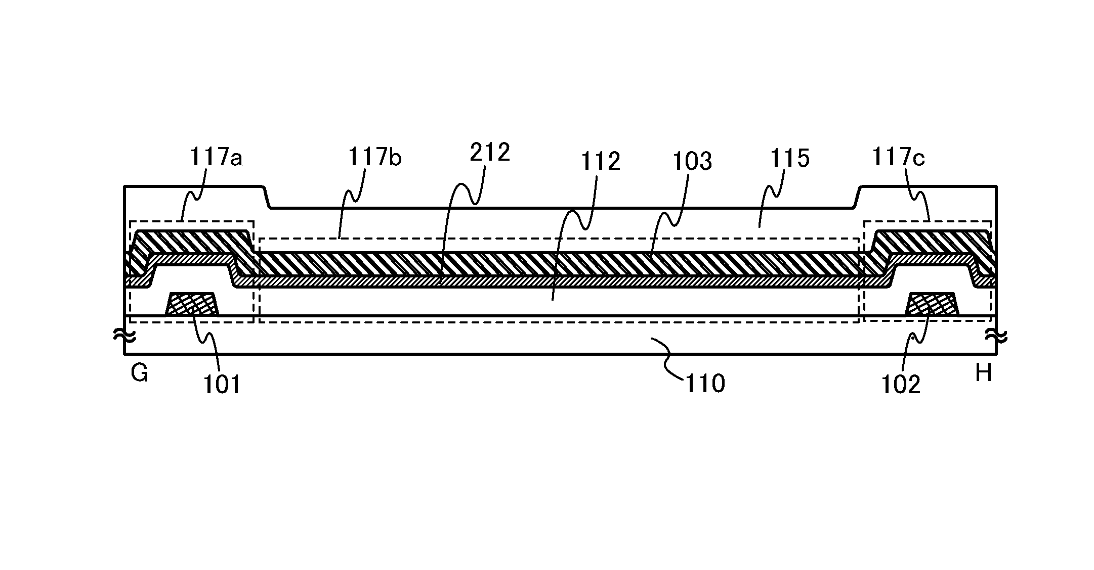
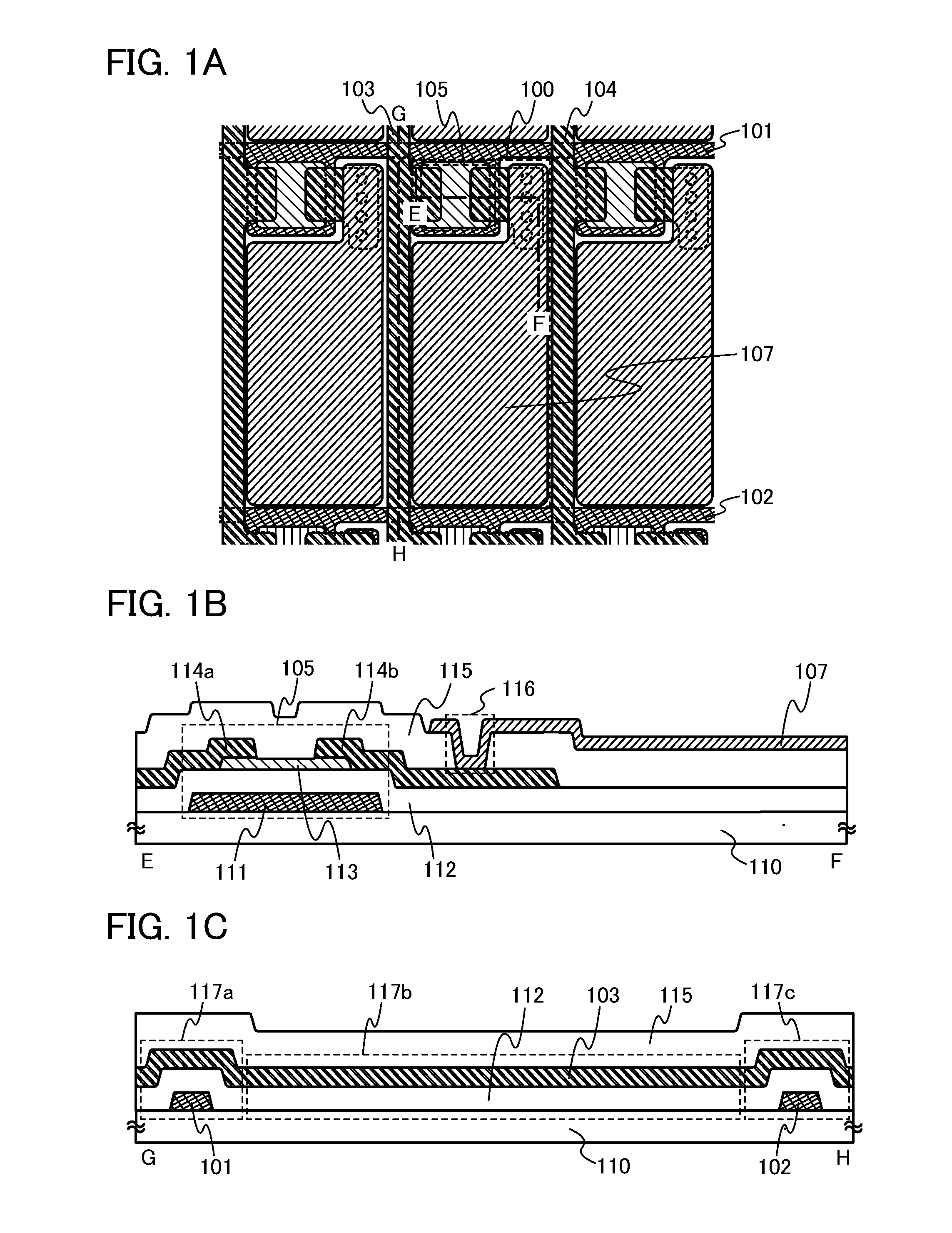
[0033]First, an example of a structure of a pixel included in a liquid crystal display device of one embodiment of the present invention is described with reference to FIGS. 1A to 1C. Specifically, an example of a structure of a pixel in a liquid crystal display device having a structure in which a liquid crystal material is interposed between one substrate provided with a pixel electrode and the other substrate provided with a counter electrode (a liquid crystal display device in w...


PUM


Abstract

An object is to reduce parasitic capacitance of a signal line included in a liquid crystal display device. A transistor including an oxide semiconductor layer is used as a transistor provided in each pixel. Note that the oxide semiconductor layer is an oxide semiconductor layer which is highly purified by thoroughly removing impurities (hydrogen, water, or the like) which become electron suppliers (donors). Thus, the amount of leakage current (off-state current) can be reduced when the transistor is off. Therefore, a voltage applied to a liquid crystal element can be held without providing a capacitor in each pixel. In addition, a capacitor wiring extending to a pixel portion of the liquid crystal display device can be eliminated. Therefore, parasitic capacitance in a region where the signal line and the capacitor wiring intersect with each other can be eliminated.

Description

TECHNICAL FIELD[0001]The present invention relates to a liquid crystal display device.BACKGROUND ART[0002]Active matrix liquid crystal display devices including a plurality of pixels arranged in matrix have been widespread. In general, the pixel includes a transistor having a gate electrically connected to a scan line and a source and a drain one of which is electrically connected to a signal line, a capacitor having terminals one of which is electrically connected to the other of the source and drain of the transistor and the other of which is electrically connected to a wiring supplying a common potential (hereinafter, also referred to as a capacitor wiring), and a liquid crystal element having terminals one of which (a pixel electrode) is electrically connected to the other of the source and the drain of the transistor and the one of the terminals of the capacitor and the other of which (a counter electrode) is electrically connected to a wiring supplying a counter potential.[000...

Claims


Application Information

Patent Timeline
Patent Type & Authority Patents(United States)
IPC IPC(8): H01L31/00
CPCG02F1/136286H01L27/1244H01L29/7869H01L27/1225H01L29/45G02F2001/13606G02F2001/136295G02F1/133345H01L29/786G02F1/136295G02F1/13606H01L27/124G02F1/136227G02F1/13624G02F1/1368G02F2202/10G09G3/3622G09G2300/0426
Inventor KONDO, TOSHIKAZUKOYAMA, JUNYAMAZAKI, SHUNPEI
Owner SEMICON ENERGY LAB CO LTD
Learn More