
High sensitivity two-stage amplifier

a two-stage amplifier, high-sensitivity technology, applied in the direction of amplifier combinations, amplifiers with field-effect devices, amplifiers, etc., can solve the problems of undesirable high-sensitivity apds, more affected signals by crosstalk and dispersion, and apds that may cost up to ten times the cost, so as to achieve less phase distortion

Active Publication Date: 2013-08-13
MACOM TECH SOLUTIONS HLDG INC
View PDF74 Cites 18 Cited by
  • Summary
  • Abstract
  • Description
  • Claims
  • Application Information

AI Technical Summary

Benefits of technology

The patent describes an optical signal receiver with improved performance. The receiver includes a two stage transimpedance amplifier with reduced phase shift, delay, and distortion while maintaining or exceeding the gain specification. The receiver also includes a feedback path that connects the output of the second stage to the input of the first stage. The feedback path introduces negative feedback as compared to the input signal. The receiver further includes a single ended to differential signal conversion unit and a method for receiving and amplifying an optical signal. The technical effects of the invention include improved signal-to-noise ratios, reduced phase distortion, and improved performance of the optical signal receiver.

Problems solved by technology

In addition, at higher rates, the received signals may be more affected by crosstalk and dispersion.
However, APDs are undesirably expensive.
For example, the APD may cost up to ten times the cost of the PIN (positive-intrinsic-negative) photodiode, plus there is additional cost for the circuitry to provide and control the APD reverse-bias voltage.
Other solutions have been proposed, but these proposed solutions do not meet the design specifications, such as noise limits.
For example, people have used a three-stage CMOS inverter approach, but this approach has limited sensitivity.

Method used


Image

  • High sensitivity two-stage amplifier
  • High sensitivity two-stage amplifier
  • High sensitivity two-stage amplifier

Examples


Embodiment Construction

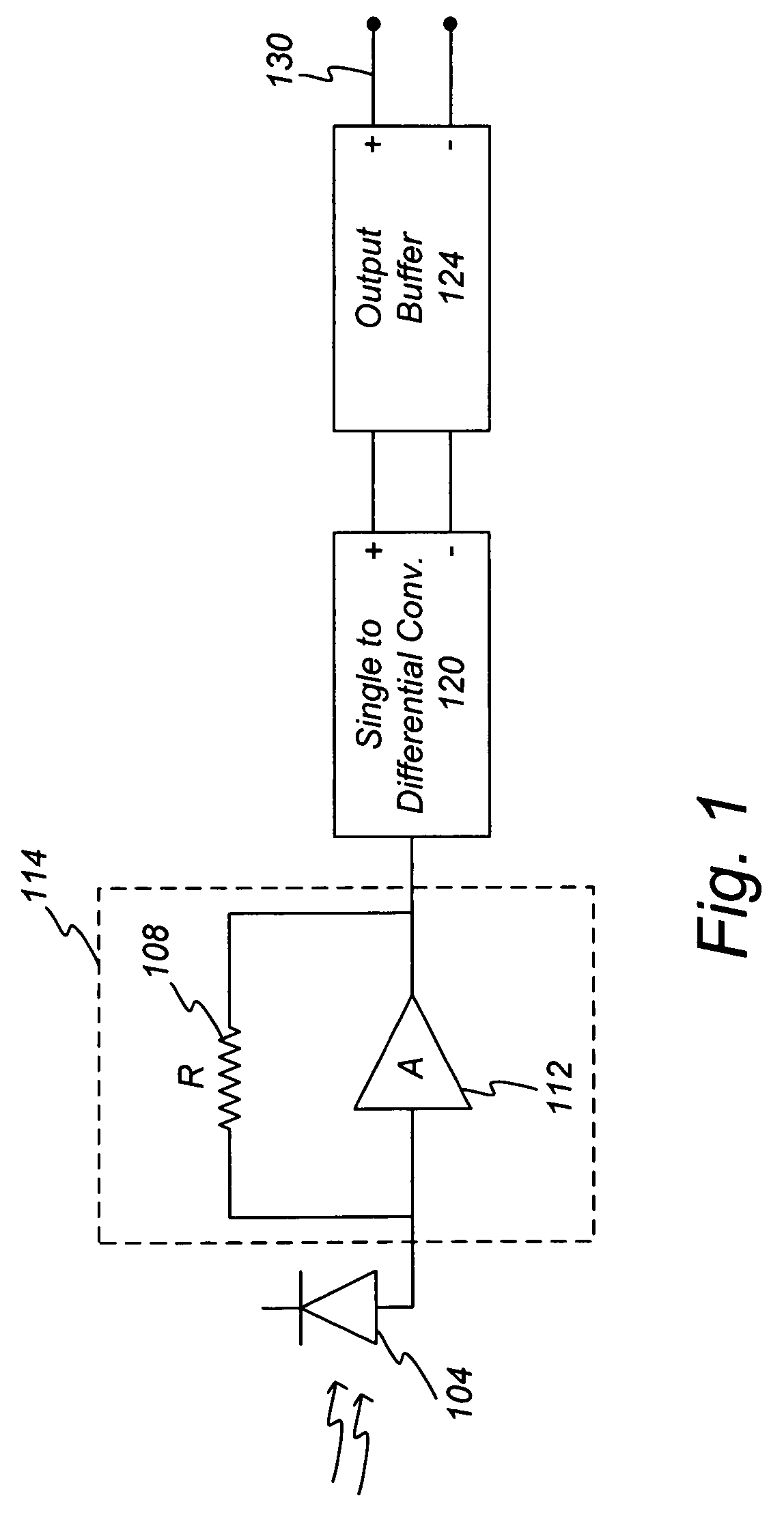
[0018]FIG. 1 illustrates an example environment of use of the invention. This is but one possible example environment of use and as such, it is contemplated that the invention may also be enabled in other environments. As shown, an amplifier (A) 112 as disclosed herein is utilized in an optical communication system. As is generally understood the amplifier 112 and a resistor 108 may comprise a TIA 114 which serves as a highly sensitive amplifier to receive and amplify weak signals in a highly accurate and noise minimized manner.

[0019]In this example environment, an optical signal is presented to a photo diode 104. In this embodiment the optical signal travels through an optical fiber (not shown) which is part of a communication system and configured to carry communication signals to the system of FIG. 1. The output of the photodiode 104 connects to the amplifier A 112 as shown. The feedback resistor R 108 provides attenuated feedback to enable desired operation. The amplifier A 112 ...


PUM


Abstract

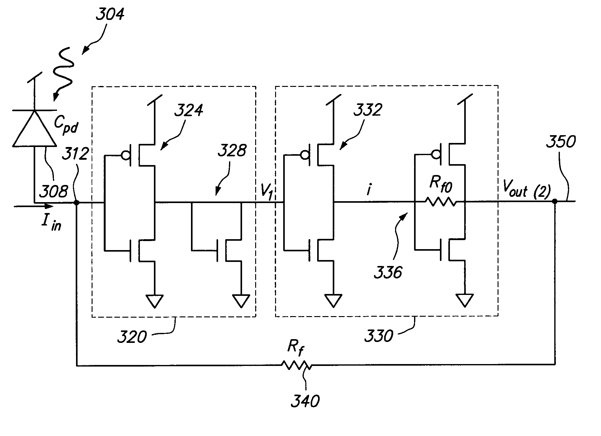
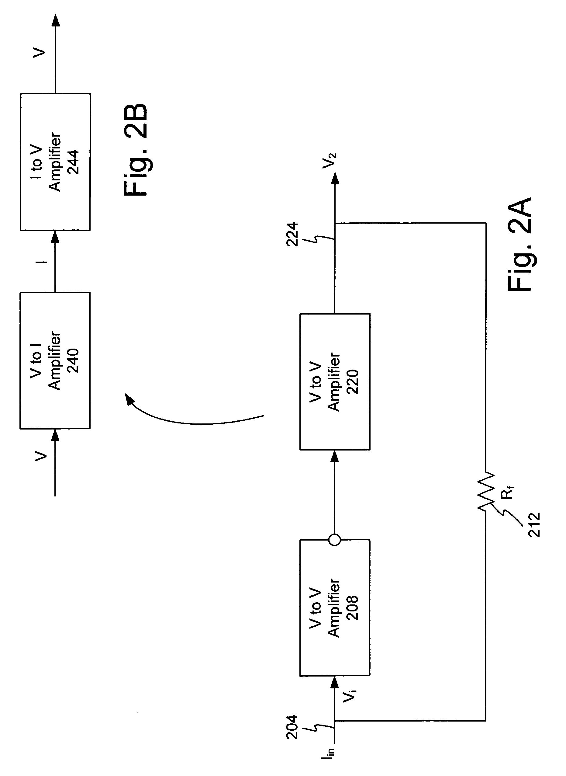
The invention relates to amplifiers and in particular, to a transimpedance amplifier for high rate applications. Disclosed is a two stage transimpedance amplifier having a first stage comprising an amplifier and a load and a second stage comprising an amplifier and a resistor. Negative feedback is provided through a feedback resistor. Only two voltage conversions occur which reduces phase distortion, as compared to three stage transimpedance amplifiers which perform 3 voltage conversions.

Description

1. PRIORITY CLAIM[0001]This application claims priority to and the benefit of U.S. Provisional Application No. 61 / 000,524 entitled HIGH SENSITIVITY TWO-STAGE CMOS TRANSIMPEDANCE AMPLIFIER FOR 1-4 GBPS APPLICATIONS which was filed on Oct. 26, 2007.2. FIELD OF THE INVENTION[0002]The invention relates to amplifiers and in particular, to a transimpedance amplifier for high rate applications.3. RELATED ART[0003]The designers of data communication systems continually strive to increase a communication system's data transmit rate, effective transmit distance, and accuracy of operation. One aspect that controls the communication systems data transmit distance is the sensitivity of the receiver. While particularly important in the optical signal communication, these principles also apply for wire line applications.[0004]As transmitted signals advance through a channel, such signals become attenuated. In addition, at higher rates, the received signals may be more affected by crosstalk and dis...

Claims


Application Information

Patent Timeline
Patent Type & Authority Patents(United States)
IPC IPC(8): H03F1/34H03F3/68
CPCH03F3/082
Inventor ZOU, HEHONGSHIVARAM, KRISHNADRAPER, DANIEL
Owner MACOM TECH SOLUTIONS HLDG INC
Learn More