

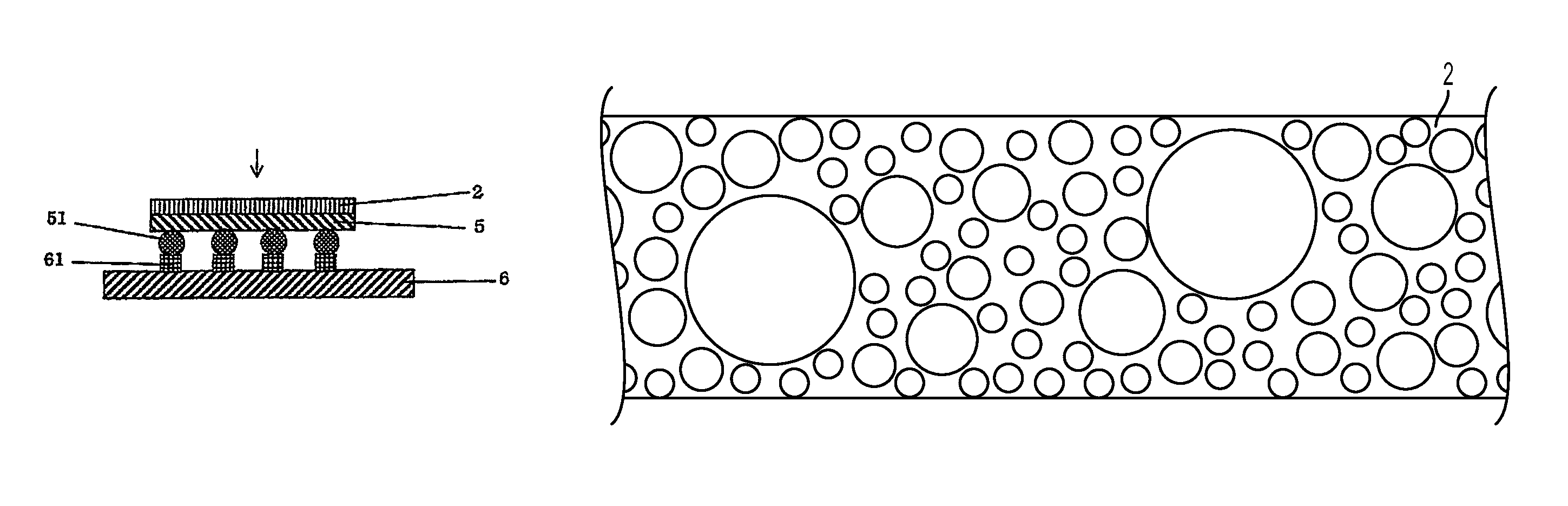
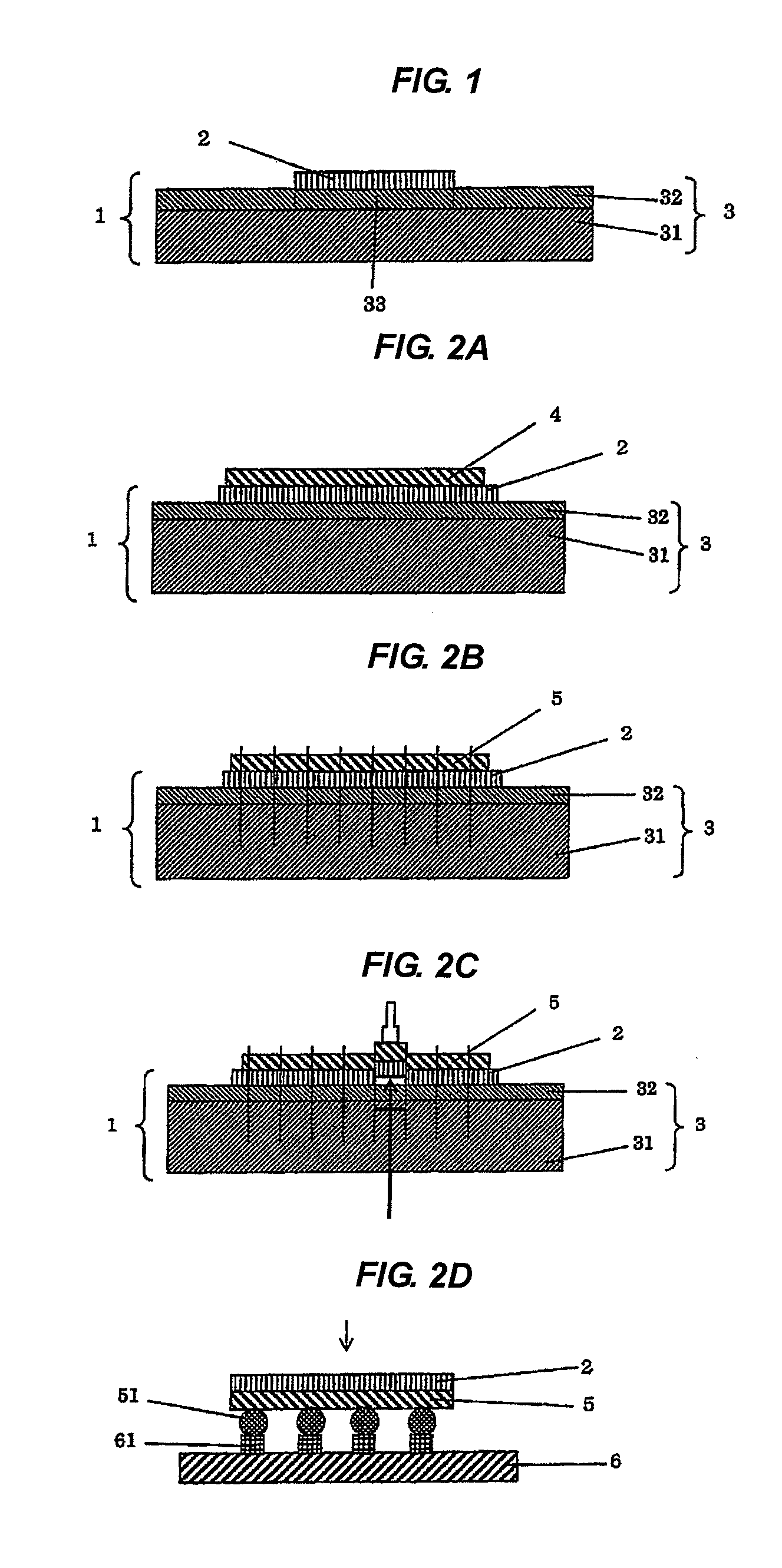
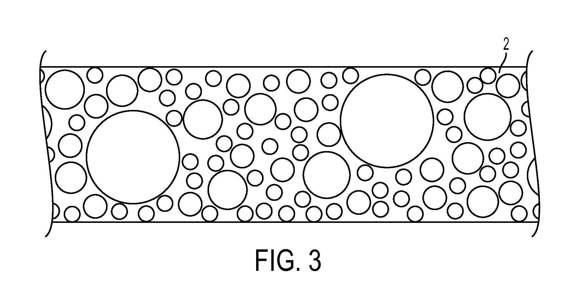
Film for flip chip type semiconductor back surface containing thermoconductive filler
a technology of thermoconductive filler and film, which is applied in the field of to dicing tapeintegrated film for flip chip type semiconductor back surface, can solve the problems of film adhesiveness to semiconductor wafers etc., the film the adhesive may be less flexible, etc., to achieve excellent heat radiation capability, high thermal conductivity of thermoconductive filler, and excellent heat radiation capability
- Summary
- Abstract
- Description
- Claims
- Application Information
AI Technical Summary
Benefits of technology
Problems solved by technology
Method used
Image

Examples
example 1
[0144]40 parts of a phenoxy resin (trade name “EP4250” manufactured by JER Co., Ltd.), 129 parts of a phenolic resin (trade name “MEH-8320” manufactured by Meiwa Chemical Co., Ltd.), 1521 parts of an alumina filler (trade name “ALMEK30WT%-N40” manufactured by CIK Nanotec Co. Ltd., having an average particle size of 0.35 μm, a maximum particle size of 3.0 μm and a thermal conductivity of 40 W / mK), 14 parts of a dye (trade name “OIL BLACK BS” manufactured by Orient Chemical Industries Co., Ltd.), and 1 part of a curing catalyst (trade name “2PHZ-PW” manufactured by Shikoku Chemical Co., Ltd.) based on 100 parts of an epoxy resin (trade name “HP4032D” manufactured by DIC Co., Ltd.) were dissolved in methyl ethyl ketone to prepare a solution of a resin composition having a solid concentration of 23.6% by weight (this may be referred to as “resin composition solution A”).
[0145]The resin composition solution A prepared as above was applied onto a releasably treated film, as a release line...
example 2
[0146]40 parts of a phenoxy resin (trade name “EP4250” manufactured by JER Co., Ltd.), 129 parts of a phenolic resin (trade name “MEH-8320” manufactured by Meiwa Chemical Co., Ltd.), 676 parts of an alumina filler (trade name “ALMEK30WT%-N40” manufactured by CIK Nanotec Co. Ltd., having an average particle size of 0.35 μm, a maximum particle size of 3.0 μm and a thermal conductivity of 40 W / mK), 14 parts of a dye (trade name “OIL BLACK BS” manufactured by Orient Chemical Industries Co., Ltd.), and 1 part of a curing catalyst (trade name “2PHZ-PW” manufactured by Shikoku Chemical Co., Ltd.) based on 100 parts of an epoxy resin (trade name “HP4032D” manufactured by DIC Co., Ltd.) were dissolved in methyl ethyl ketone to prepare a solution of a resin composition having a solid concentration of 23.6% by weight (this may be referred to as “resin composition solution B”).
[0147]The resin composition solution B prepared as above was applied onto a releasably treated film, as a release liner...
PUM
| Property | Measurement | Unit |
|---|---|---|
| Ra | aaaaa | aaaaa |
| particle size | aaaaa | aaaaa |
| particle size | aaaaa | aaaaa |
Abstract
Description
Claims
Application Information