Memory switching control apparatus using open serial interface, operating method thereof, and data storage device therefor

a control apparatus and serial interface technology, applied in the direction of digital transmission, generating/distributing signals, instruments, etc., can solve the problems of difficult synchronization between data and the clock, the probability of data and data occurrence problems is relatively high, and the conventional parallelized memory interface has a limitation to the highest speed, so as to reduce the complexity of design and implementation of the memory interface, the effect of preventing data and data input/output delays

Inactive Publication Date: 2013-12-17
ELECTRONICS & TELECOMM RES INST
View PDF17 Cites 14 Cited by
  • Summary
  • Abstract
  • Description
  • Claims
  • Application Information

AI Technical Summary

Benefits of technology

[0017]The present invention provides a memory switching control apparatus using an open serial interfacing scheme and an operating method thereof, capable of preventing a bottle neck of data and data input / output delays associated with using of a plurality of data storage devices and of reducing a complexity in design and implementation of the memory interface.
[0019]The present invention also provides a memory switching control apparatus using an open serial interfacing scheme and an operating method thereof, capable of preventing any one of the requests from being delayed or canceled in a case where a request of a main processing unit for a usage right to a memory and a request of an IO interface to the memory are simultaneously issued.
[0020]The present invention also provides a memory switching control apparatus using an open serial interfacing scheme and an operating method thereof, capable of enhancing flexibility, reliability, availability, and performance in data communication processes between a memory and a processing unit by facilitating connection between different types of data storage devices in the same standard of a serial interfacing scheme, facilitating independent input and output of data through respective memory interfacing ports, and facilitating changing positions of addressing spaces of the memory interfacing ports, and facilitating changing widths of serial interfacing lines.

Problems solved by technology

Particularly, in an embedded system and a server system requiring high availability, a probability of occurrence of problems in the data storage device is relatively high in comparison with other devices.
However, a conventional parallelized memory interface has a limitation to a highest speed since the memory interface is implemented on a printed circuit board (PCB).
In addition, since a high-frequency-band clock is included in the parallelized memory interface, synchronization between data and the clock is a difficult task.
In addition, since signal characteristics may be slightly varied according to heat, physical impact, vibration, and the like, the synchronization between parallel data and between the data and clock may be unstable or broken down.
However, due to the limitation of existing parallelized memory interface scheme, difficulty in design of the memory interface is still remained and increased.
In addition, in case of using a plurality of data storage devices, it is difficult to prevent a bottle neck of data and data input / output delays by using a memory interfacing scheme using a single interface unit.
Even in case of using the aforementioned parallelized memory interface scheme, since different interfaces need to be used for different types of memory devices, a complexity in design and implementation of the memory interfaces and the number of pins are increased.
Therefore, when a memory interface or a memory connected to the memory interface is in disorder, the processing unit cannot operate, so that the entire system may be stopped.

Method used


Image

  • Memory switching control apparatus using open serial interface, operating method thereof, and data storage device therefor
  • Memory switching control apparatus using open serial interface, operating method thereof, and data storage device therefor
  • Memory switching control apparatus using open serial interface, operating method thereof, and data storage device therefor

Examples


Embodiment Construction

[0041]Hereinafter, embodiments of the present invention will be described in detail with reference to the accompanying drawings. For clarifying the present invention, detailed description of well-known functions and constructions will be omitted. In the accompanying drawing, elements having similar functions and operations are denoted by the same reference numerals.

[0042]In the specification, “connection between an element and another element” includes “indirect connection through still another element therebetween” as well as “direct connection therebetween”. In addition, “comprising an element” denotes not excluding other elements but further comprising other elements if there is no specific contrary description.

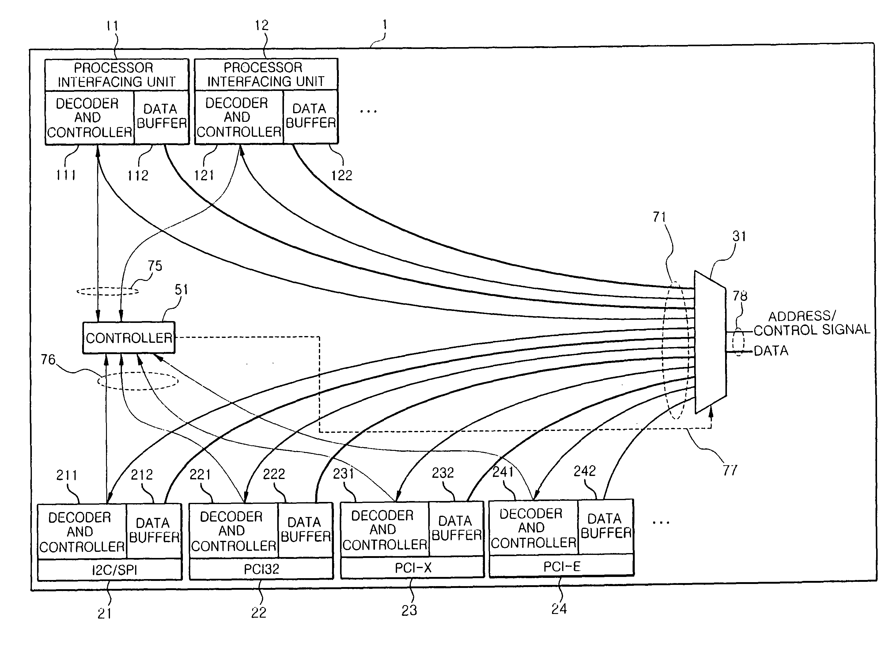
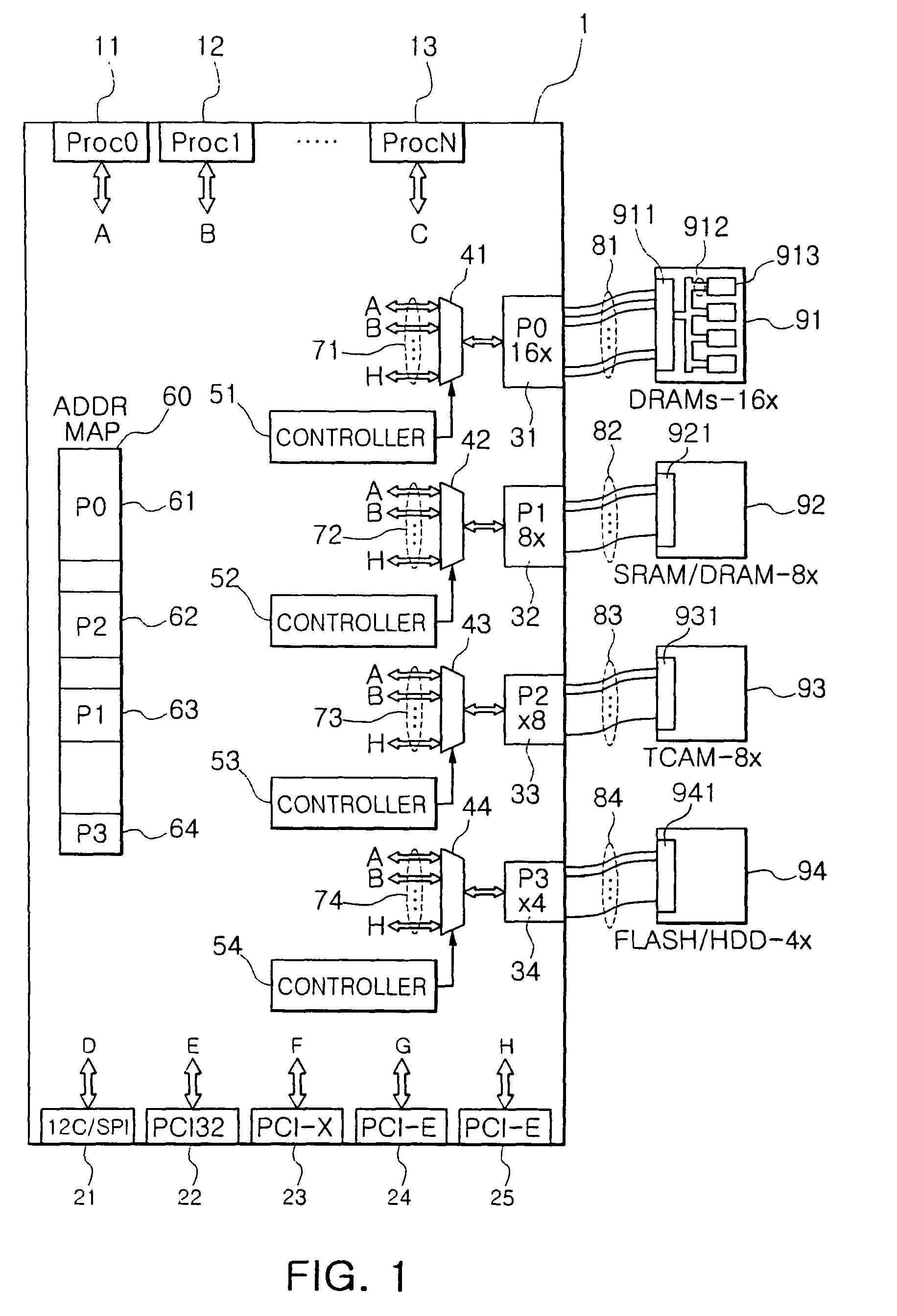
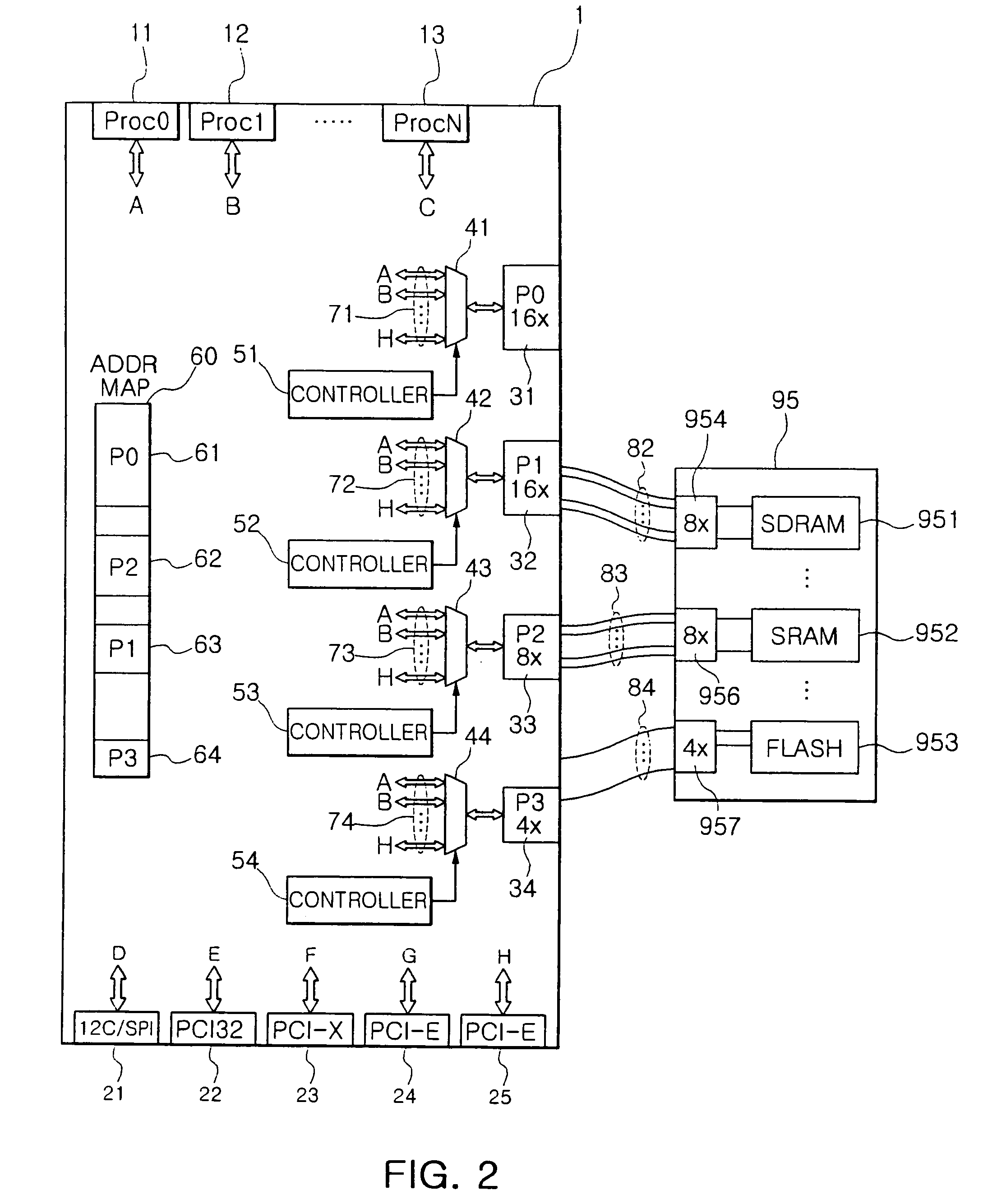
[0043]In a memory switching control apparatus according to the present invention, independent memory interfacing ports and arbitration units are provided so as to arbitrate connection between one or more data storage device including memory and one or more processing units...


PUM


Abstract

Provided is a memory switching control apparatus using an open serial interfacing scheme capable of enhancing flexibility, reliability, availability, performance in a data communication processes between a memory and a processing unit and an operating method thereof. The memory switching control apparatus includes: one or more processor interfacing units which perform interfacing with one or more processing units; one or more memory interfacing units which have open-serial-interfacing-scheme memory interfacing ports to interface with data storage devices connected to the memory interfacing ports in a serial interfacing scheme; and a plurality of arbitrating units which are provided corresponding to the memory interfacing units to independently arbitrate usage rights of the processor interfacing units to the memory interfacing units.

Description

CROSS-REFERENCE TO RELATED APPLICATIONS[0001]This application claims the priority of Korean Patent Application No. 10-2007-0096879 filed on Sep. 21, 2007, in the Korean Intellectual Property Office, the disclosure of which is incorporated herein by reference.BACKGROUND OF THE INVENTION[0002]1. Field of the Invention[0003]The present invention relates to a memory switching control apparatus using open serial interfacing capable of enhancing flexibility, reliability, availability, and performance in a data communication processes between a memory and a processing unit and an operating method thereof.[0004]The present invention is derived from a research project supported by the IT R&D program of MIC / IITA [2006-S-061-02, IPv6-Based QoS Service and Terminal Mobility Supporting Router Technology].[0005]2. Description of the Related Art[0006]In general, an apparatus including processing units such as personal computers (PC), embedded systems, and portable apparatuses such as mobile phones...

Claims


Application Information

Patent Timeline
Patent Type & Authority Patents(United States)
IPC IPC(8): G06F13/14G06F12/00G06F13/00
CPCG06F12/0646G06F13/1657G06F13/14
Inventor KIM, BUP JOONGCHOI, WOO YOUNGNAM, KOOK JINAHN, BYUNG JUN
Owner ELECTRONICS & TELECOMM RES INST
Why Eureka
Try Eureka