
Laminate constructs for micro-fluid ejection devices

a technology of ejection device and microfluid, which is applied in the direction of semiconductor devices, printing, inking apparatus, etc., can solve the problems of reducing the size of substrates that can be fabricated, reducing the size of substrates, and reducing so as to reduce the cost of ceramic components and minimize the challenges of attaching pcbs , the effect of avoiding thermal curing stresses

Active Publication Date: 2014-01-07
FUNAI ELECTRIC CO LTD
View PDF10 Cites 1 Cited by
  • Summary
  • Abstract
  • Description
  • Claims
  • Application Information

AI Technical Summary

Benefits of technology

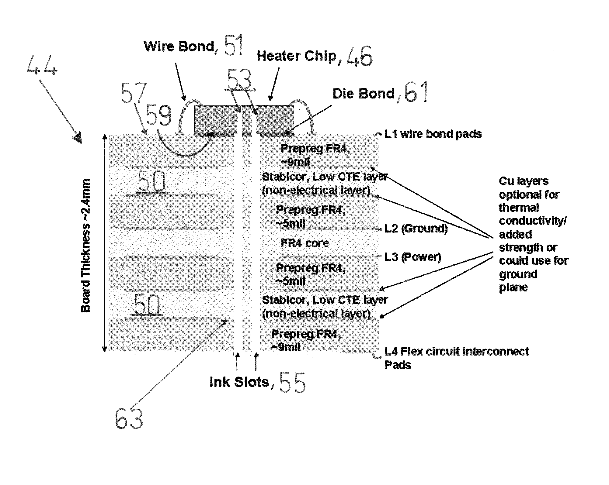
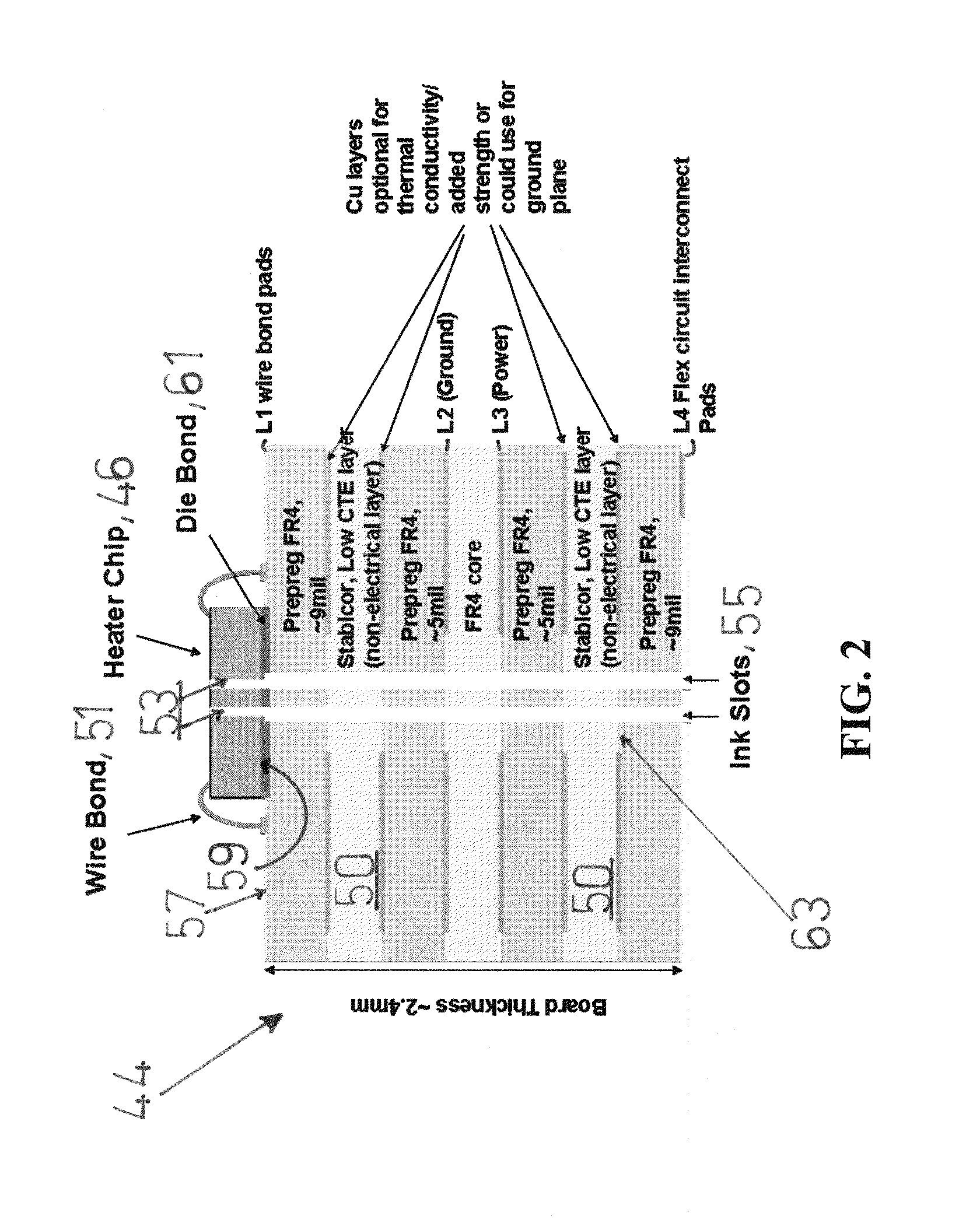
The invention proposes a new way to design micro-fluid ejection heads. By combining the ceramic base with the electrical function of a printed circuit board, it eliminates the expensive ceramic component and minimizes challenges in attaching printed circuits. This laminate construct also avoids thermal curing stresses on the printed circuit board. The ejection head is designed without sacrificing its CTE match, stiffness, and thermal conductivity by utilizing carbon fiber PCB laminate technology. This approach provides a more extendible and cost-effective solution for larger and page-wide ejection heads.

Problems solved by technology

Notwithstanding these advantages, ceramics have known drawbacks.
Tape cast varieties, however, are relatively expensive to fabricate and each comes with challenges in selecting compatibility relative to other materials.
Three, there exists a practical limitation in the sizes of substrates that can be fabricated due to corresponding limitations in the sizes of modern presses.
Naturally, this creates problems for manufacturers seeking to increase dimensions in printing swaths and chip arrays.
However, there remains limits and unresolved process challenges as will be seen.
It also limits the space to add a protective FR4 layer to the bottom of the board, such as over trace areas so that the only exposed metal on the bottom is for flexible cable attachment pads.
By allowing a thicker die, on the other hand, the board thickness can increase but at an adverse cost to the substrate of poorer thermal dissipation.
However, since the boards are thin and flexible, they tend to warp after fabrication.
This not only presents challenges for attaching the board to the ceramic, but compromises corrosion protection for the traces.
Still other problems associated with board-to-ceramic attachment include: 1) squeezing epoxy excesses into the chip pocket causing, thereby interfering with later die mounting or contributing to volume variability in the pocket and making encapsulation heights unpredictable; or 2) creating interfacial voids that allow ink to access the delicate wiring traces on the bottom of the board.
Alignment or registration between the board and ceramic has also resulted in manufacturing concerns.
One, the board warping makes it difficult to properly register components.
Two, routing tolerances on the board provide little room to adjust components.
As ejection heads move beyond single- or double-chip heads to larger arrays, the weight of now larger ceramics becomes problematic for smaller pick-and-place tools.
However, UV curing lamps and other gluing fixtures are difficult to incorporate into standard tooling.
Neither of these, however, concern themselves with the challenges associated with precision methods needed to attach silicon inkjet chips to PCB materials.
Rather, they relate to using conventional PCB material sets, which are insufficient for modern concerns.
Typical FR4 PCB materials, however, have CTEs of ˜16-20 ppm / ° C. and represent poor substrates for attachment to silicon chips having CTEs of 2-4 ppm / ° C. While ceramic materials with CTEs of 6-8 ppm / ° C. are a better match, they suffer the problems identified above.
Also, standard FR4 based circuit boards may not provide enough rigidity / stiffness for micro-fluid applications.
In turn, mounting a board assembly to a printhead body can induce significant stresses that may translate into deformation where the die interfaces with the FR4 substrate.
˜25 W / mK), and this could prove challenging for dissipating heat generated during printing.
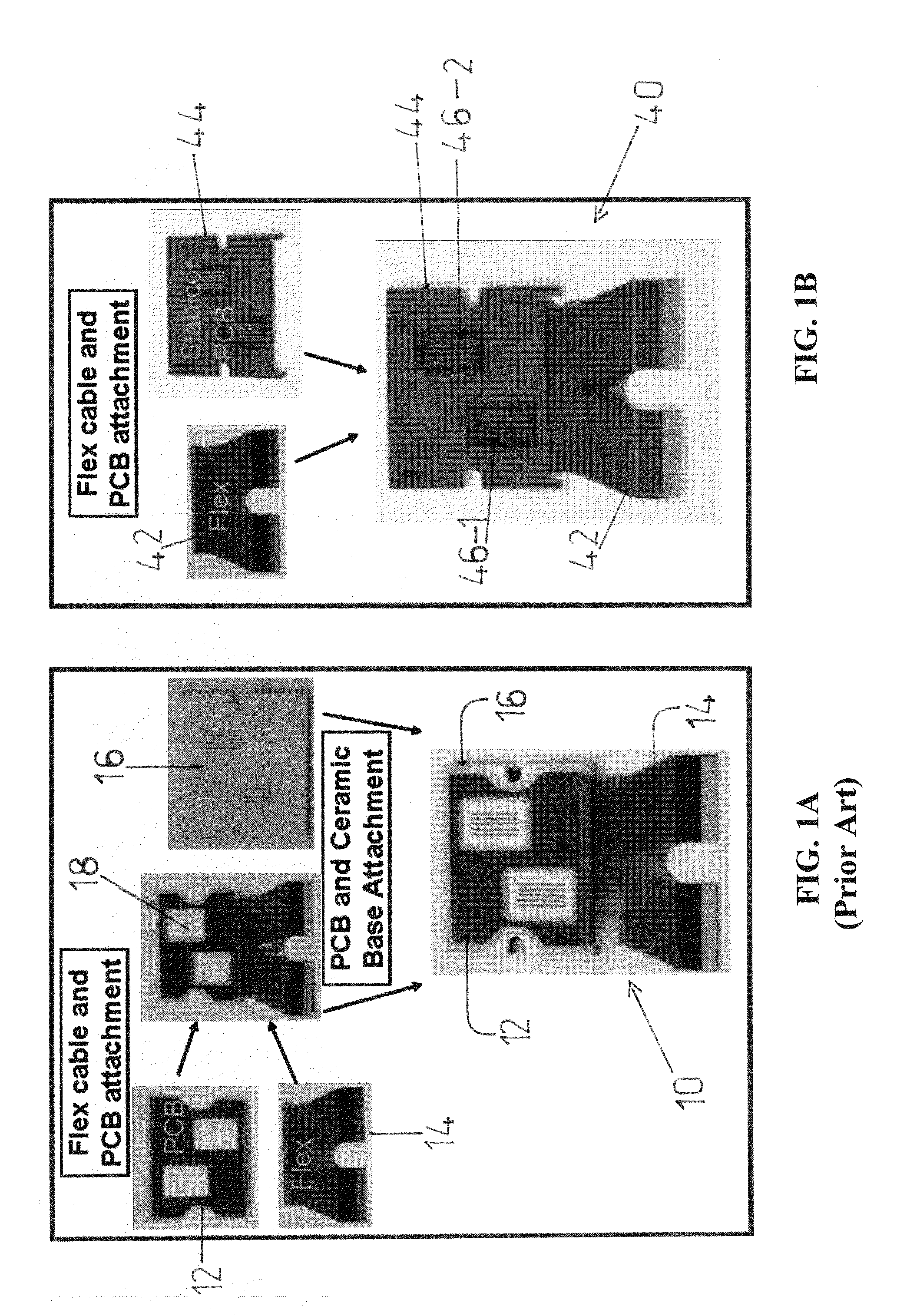
Unfortunately, the printed circuit board 24 and ceramic base substrate 30 cause the design to encounter much of the same problems earlier described.

Method used


Image

  • Laminate constructs for micro-fluid ejection devices
  • Laminate constructs for micro-fluid ejection devices
  • Laminate constructs for micro-fluid ejection devices

Examples


example

[0036]As an initial proof of concept, the inventors have mounted dies on several Stablcor layers of the above construction using the same die bond material, dispense, and pick-and-place processes used on conventional ceramic substrate designs. Thickness were somewhat arbitrarily set and design and process conditions were not optimized for planarity in the chip pocket area. Result: Y-axis chip bows were observed at less than 5 μm over a ½ inch chip length. While such is not as good as the 1-2 μm achieved on ceramic substrates, it is considerably better than the 15-16 μm achieved on other designs (not shown). It is believed that with the optimization of planarity between the chip and laminate construct, results will be further improved.

[0037]With reference to FIGS. 5-9, the laminate construct 44 is further useful in overcoming the disadvantages of the design in FIG. 4 (prior art). In all such embodiments, the laminate constructs are intended to provide fluidic and electrical interconn...


PUM


Abstract

A micro-fluid ejection head has an ejection chip to expel fluid. It connects to a laminate construct. The construct has vertically configured wiring layers interspersed with non-wiring layers, such as carbon fiber layers. An upper of the wiring layers electrically connects to the ejection chip. The upper layer may also support a planar undersurface of the chip directly on a surface or in a recessed pocket. The two can connect with a die bond, such as one having silica or boron nitride. Fluid connections exist between ink feed slots of the chip and the laminate construct. A silicon tile or other material may also fluidly interconnect with the two. A plastic manifold optionally supports the laminate construct and may fluidly connect to it. The wiring layers of the laminate contemplate ground, power, and various bond pads. Other construct layers contemplate prepreg or core FR4 layers.

Description

FIELD OF THE INVENTION[0001]The present invention relates to micro-fluid ejection devices, such as printers, copiers, graphics plotters, all-in-ones, etc. More particularly, it relates to laminate constructs serving multiple functions that minimize the number of components, processing steps and size required for ejection heads, e.g., inkjet printheads.BACKGROUND OF THE INVENTION[0002]The art of printing images with micro-fluid technology is relatively well known. A conventional permanent or semi-permanent ejection head has access to a local or remote supply of fluid. The fluid ejects from an ejection zone of the head to a print media in a pattern corresponding to pixels of images being printed. Over time, the heads and fluid drops have become smaller.[0003]As part of recent trends, manufacturers increasingly have placed their inkjet ejection chips on ceramic substrates. Ceramics are relatively high modulus materials offering low coefficients of thermal expansion (CTEs). They are kno...

Claims


Application Information

Patent Timeline
Patent Type & Authority Patents(United States)
IPC IPC(8): B41J2/045
CPCB41J2/1632B41J2/1601B41J2/1634B41J2/1623B41J2/1643B41J2/1626B41J2/14072B41J2202/20B41J2/14H01L2224/48091H01L2224/73265H01L2924/10155H01L2924/00014B41J2/1433B41J2002/14419B41J2002/14491
Inventor ANDERSON, FRANK EDWARDCORLEY, RICHARDDIXON, MICHAEL JOHNFANG, JIANDONGSALDANHA SINGH, JEANNE MARIE
Owner FUNAI ELECTRIC CO LTD
Learn More