Method of forming three dimensional integrated circuit devices using layer transfer technique

a layer transfer and integrated circuit technology, applied in the field of three-dimensional integrated circuit devices and fabrication methods, can solve the problems of many barriers to practical implementation of 3d stacked chips, wires that connect together transistors degrade in performance with scaling, and many wires dominate performance, functionality and power consumption of ics

Active Publication Date: 2014-02-04
MONOLITHIC 3D
View PDF570 Cites 49 Cited by
  • Summary
  • Abstract
  • Description
  • Claims
  • Application Information

AI Technical Summary

Problems solved by technology

However, wires (interconnects) that connect together transistors degrade in performance with “scaling”.
The situation today may be that wires dominate performance, functionality and power consumption of ICs.
However, there are many barriers to practical implementation of 3D stacked chips.
Copper or Aluminum wiring levels, in fact, can get damaged when exposed to temperatures higher than ˜400° C. If one would like to arrange transistors in 3 dimensions along with wires, it has the challenge described below.
When the Top Transistor Layer may be constructed using Temperatures higher than 700° C., it can damage the Bottom Wiring Layer.Due to the above mentioned problem with forming transistor layers above wiring layers at temperatures lower than 400° C., the semiconductor industry has largely explored alternative architectures for 3D stacking.
Unfortunately, the size of Contacts to the other Layer may be large and the number of these Contacts may be small.
This low connectivity between layers may be because of two reasons: (i) Landing pad size needs to be relatively large due to alignment issues during wafer bonding.
Etching deep holes in silicon with small lateral dimensions and filling them with metal to form TSVs may be not easy.
Therefore, connectivity between two wafers may be limited.
Unfortunately, however, almost all semiconductor devices in the market today (logic, DRAM, flash memory) utilize horizontal (or planar) transistors due to their many advantages, and it may be difficult to convince the industry to move to vertical transistor technology.
A process flow may be utilized to transfer this top transistor layer atop the bottom wiring and transistor layers at temperatures less than 400° C. Unfortunately, since transistors are fully formed prior to bonding, this scheme suffers from misalignment issues.
While Topol describes techniques to reduce misalignment errors in the above paper, the techniques of Topol still suffer from misalignment errors that limit contact dimensions between two chips in the stack to >130 nm.
Unfortunately, however, these technologies have higher defect density compared to standard single crystal silicon.
This higher defect density degrades transistor performance.
However, the approach described by Hubert has some challenges including the use of difficult-to-manufacture nanowire transistors, higher defect densities due to formation of Si and SiGe layers atop each other, high temperature processing for long times, and difficult manufacturing.
None of these products are true 3DICs.
In particular, yield and reliability of extremely complex three dimensional systems will have to be addressed, particularly given the yield and reliability difficulties encountered in complex Application Specific Integrated Circuits (ASIC) built in recent deep submicron process generations.
However, wires (interconnects) that connect together transistors degrade in performance with “scaling”.
The situation today may be that wires dominate performance, functionality and power consumption of ICs.
Irrespective of the technique used to construct 3D stacked integrated circuits or chips, heat removal may be a serious issue for this technology.
Removing the heat produced due to this power density may be a significant challenge.
In addition, many heat producing regions in 3D stacked integrated circuits or chips have a high thermal resistance to the heat sink, and this makes heat removal even more difficult.

Method used


Image

  • Method of forming three dimensional integrated circuit devices using layer transfer technique
  • Method of forming three dimensional integrated circuit devices using layer transfer technique
  • Method of forming three dimensional integrated circuit devices using layer transfer technique

Examples


Embodiment Construction

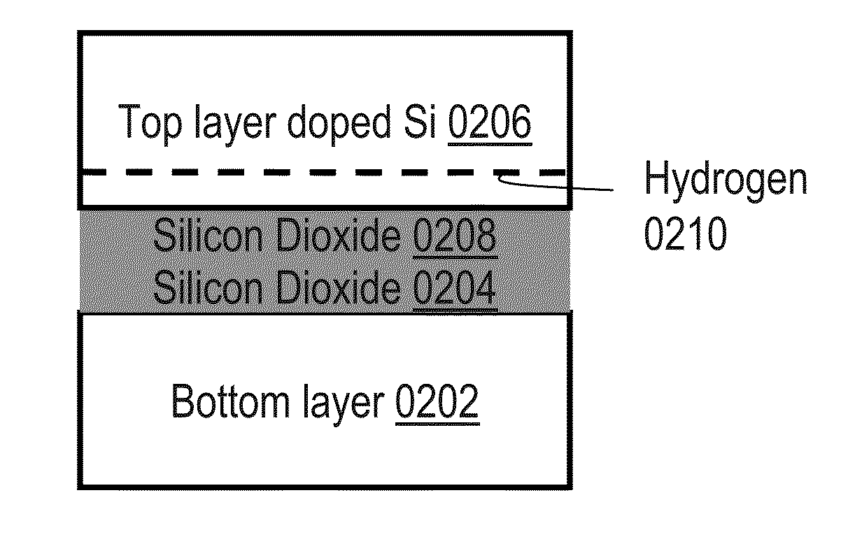
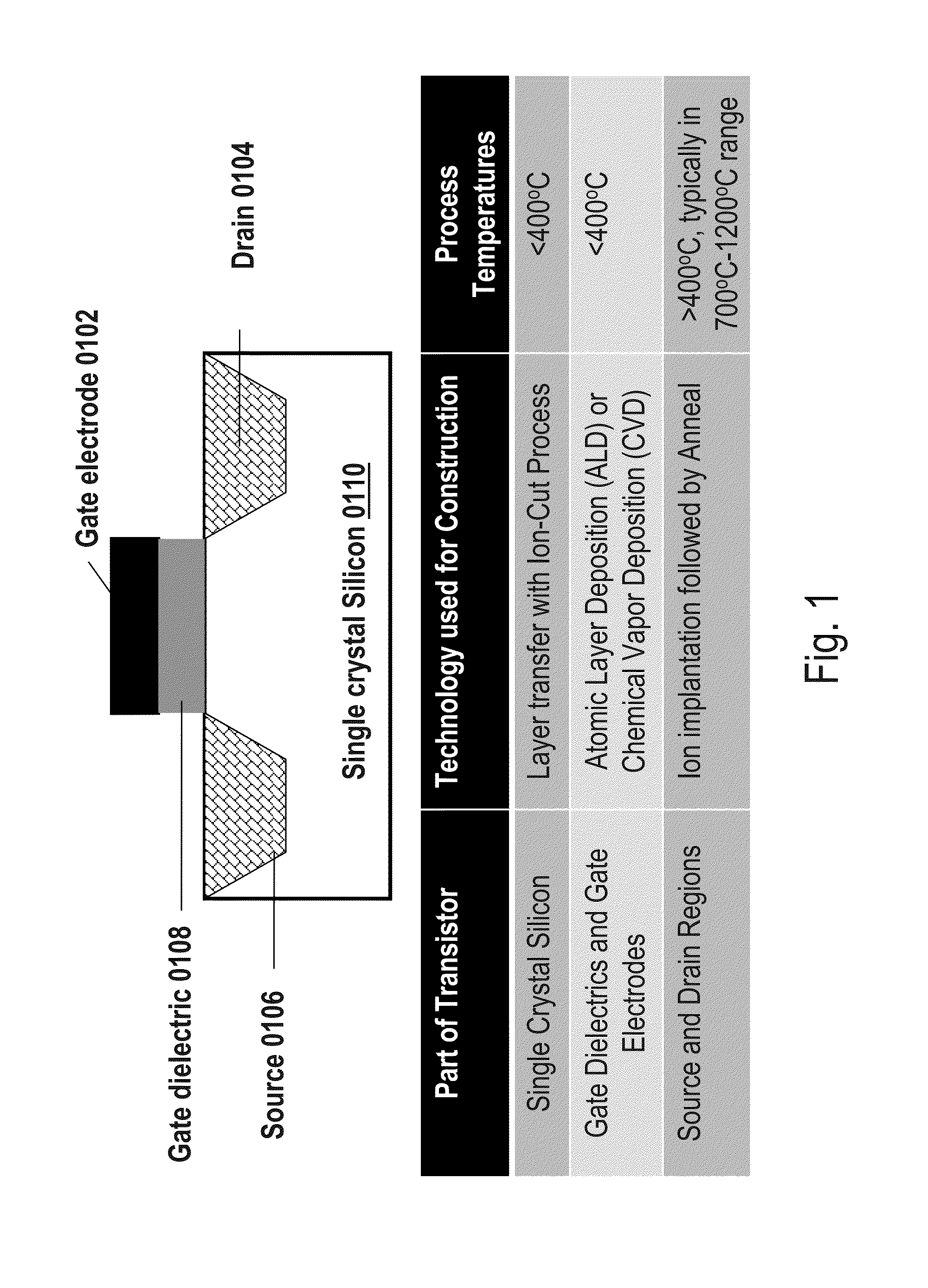
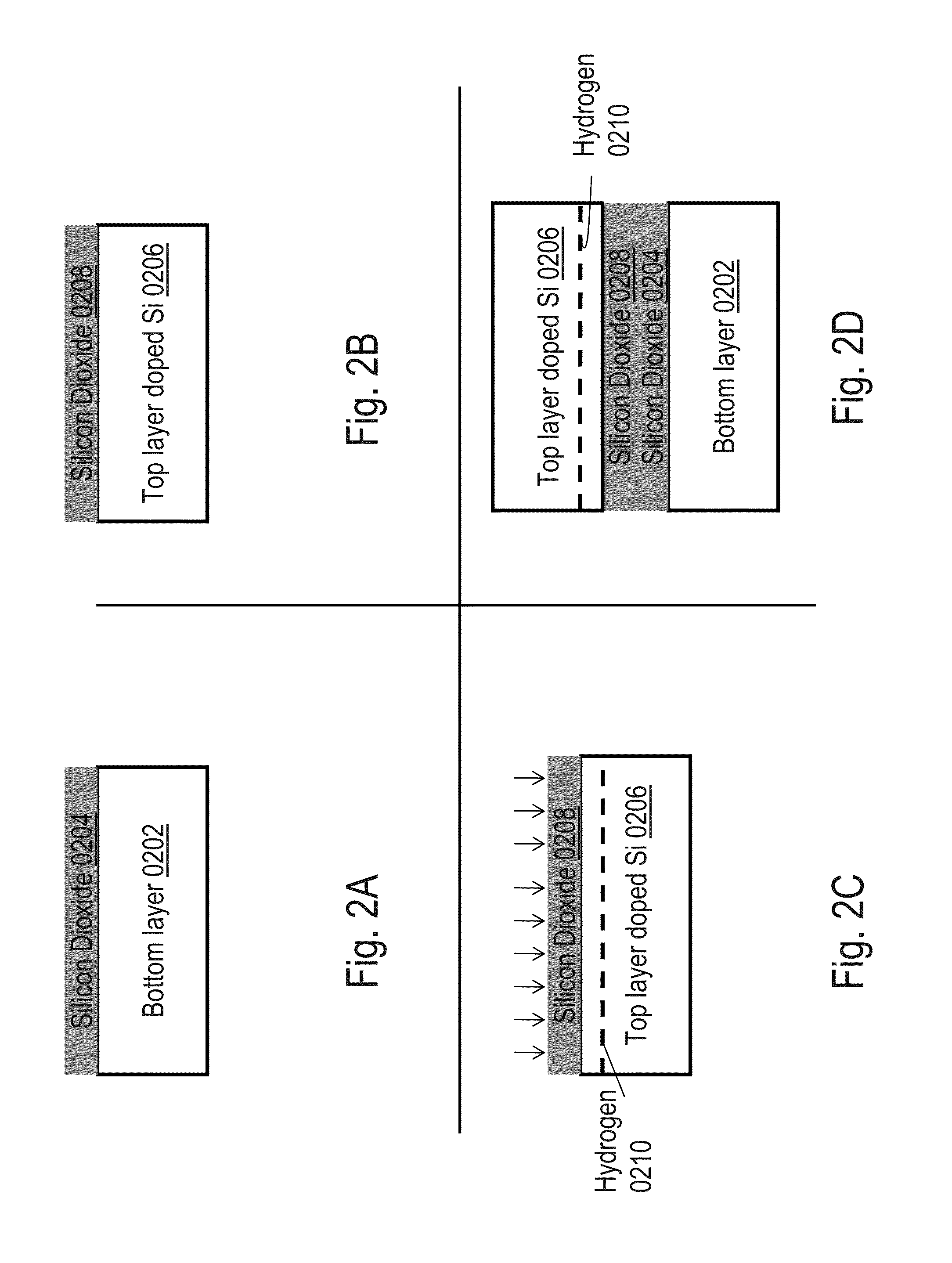
[0232]Embodiments of the invention are now described with reference to FIGS. 1-148, it being appreciated that the figures illustrate the subject matter not to scale or to measure. Many figures describe process flows for building devices. These process flows, which are essentially a sequence of steps for building a device, have many structures, numerals and labels that are common between two or more adjacent steps. In such cases, some labels, numerals and structures used for a certain step's figure may have been described in previous steps' figures.

[0233]Embodiments of the invention are now described with reference to the drawing figures. Persons of ordinary skill in the art will appreciate that the description and figures illustrate rather than limit the invention and that in general the figures are not drawn to scale for clarity of presentation. Such skilled persons will also realize that many more embodiments are possible by applying the inventive principles contained herein and t...


PUM


Abstract

A method for formation of a semiconductor device including a first wafer including a first single crystal layer comprising first transistors and first alignment mark, the method including: implanting to form a doped layer within a second wafer; forming a second mono-crystalline layer on top of the first wafer by transferring at least a portion of the doped layer using layer transfer step, and completing the formation of second transistors on the second mono-crystalline layer including a step of forming a gate dielectric followed by second transistors gate formation step, wherein the second transistors are horizontally oriented.

Description

BACKGROUND OF THE INVENTION[0001]This application is a national stage application into the USPTO of PCT / US 2011 / 042071 of international filing date Jun. 28, 2011, of which priority to is claimed.[0002]1. Field of the Invention[0003]The invention relates to the general field of Integrated Circuit (IC) devices and fabrication methods, and more particularly to multilayer or Three Dimensional Integrated Circuit (3D-IC) devices[0004]2. Discussion of Background Art[0005]Over the past 40 years, one has seen a dramatic increase in functionality and performance of Integrated Circuits (ICs). This has largely been due to the phenomenon of “scaling” i.e. component sizes within ICs have been reduced (“scaled”) with every successive generation of technology. There are two main classes of components in Complementary Metal Oxide Semiconductor (CMOS) ICs, namely transistors and wires. With “scaling”, transistor performance and density typically improve and this has contributed to the previously-ment...

Claims


Application Information

Patent Timeline
Patent Type & Authority Patents(United States)
IPC IPC(8): H01L21/822H01L21/8238
CPCH01L21/8221H01L21/8238G11C17/14H01L21/84H01L23/36H01L23/5252H01L23/544H01L25/0657H01L21/76254H01L25/18H01L27/0207H01L27/0688H01L27/0694H01L27/092H01L27/105H01L27/10873H01L27/10876H01L27/10897H01L27/11H01L27/112H01L27/11206H01L27/11803H03K17/687H03K19/0948H03K19/17704H03K19/17756H03K19/17764H03K19/17796G11C16/0483G11C17/06G11C29/82H01L21/845H01L29/785H01L29/78696H01L21/6835H01L25/0655H01L24/16H01L24/32H01L2224/16225H01L2224/32225H01L2224/73204H01L2224/73265H01L2924/19107H01L2225/06527H01L23/481H01L24/48H01L27/1104H01L27/1108H01L2223/5442H01L2223/54426H01L2223/54453H01L2224/32145H01L2224/48091H01L2225/06517H01L2225/06589H01L2924/01019H01L2924/01066H01L2924/01322H01L2924/13091H01L2924/3011H01L2225/06513H01L2225/06541H01L2924/13062H01L2924/14H01L2924/1433H01L2924/1436H01L2924/1437H01L2224/16145H01L2224/48227H01L2924/15311H01L2924/10253H01L2924/3025H01L2924/1461H01L2924/12042H01L2924/181H01L2924/12032H01L2924/1305H01L2924/00014H01L2924/00012H01L2924/00H01L2224/45099H01L2224/45015H01L2924/207H01L23/5286H01L23/535H01L29/42392H10B12/05H10B12/053H10B12/50H10B10/125H10B10/00H10B10/12H10B20/00H10B20/20
Inventor OR-BACH, ZVISEKAR, DEEPAKCRONQUIST, BRIANWURMAN, ZE'EV
Owner MONOLITHIC 3D
Why Eureka
Try Eureka