
Algorithm of Cu interconnect dummy inserting

a technology of interconnect dummy and algorithm, which is applied in the field of algorithm of interconnect dummy inserting, can solve the problems of strong correlation between dishing defect, insurmountable difficulties in technology and integration, affecting the yield and reliability of the product, etc., and achieves better planarization effect and reasonable metal density.

Active Publication Date: 2014-02-04
SHANGHAI HUALI MICROELECTRONICS CORP
View PDF7 Cites 0 Cited by
  • Summary
  • Abstract
  • Description
  • Claims
  • Application Information

AI Technical Summary

Benefits of technology

The present invention is about a new algorithm for inserting copper interconnects. This algorithm avoids the problems with existing methods that focus on maximizing fill density. Instead, it uses reasonable metal density and line width to achieve better planarization. The combination of line width and density also helps in copper plating and chemical mechanical polishing, which affects the filling process. Overall, this new algorithm results in better quality copper interconnects.

Problems solved by technology

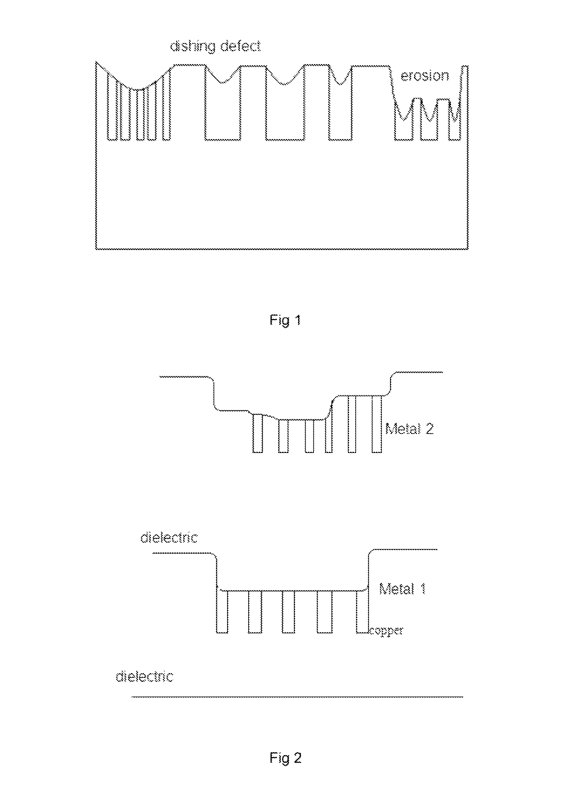
As FIG. 1 illustrated, some area such as high density area of wide line or graphics will appear in phenomenon like dishing defect or erosion, which become the serious flaws of affecting the flatness of Post-CMP.
Thereinto, the ECP profile and the grinding characteristics of CMP are directly affected by the graphical features of metal wire's area density, line width, spacing, etc, which result in the strong correlation between dishing defect of Post-CMP, erosion and graphics.
Such effect will be worse with the increase of metal layer number, which will cause insurmountable difficulties in technology and integration, and affect the yield and the reliability of the product.
The weakness of this method is that although it may improve the overall density of the metal, but it ignores some critical factor, such as the impact of the line width to the flatness after chemical snow polishing and so on, thus we can't control the variation of the thickness of the interlayer dielectric and the metal accurately.
It totally did not consider that large number of redundant metal pattern will increase the coupling capacitor of back metal layer and it may raise issues like signal delay and power consumption increase.
Model-based dummy fill method may get better effect of flatness in nanometer process node, but owing to extraction of simulation model and complicated fill algorithm, it have high requirements on events and resources which bring non-negligible negative impact to the design cycle and cost.

Method used


Image

  • Algorithm of Cu interconnect dummy inserting
  • Algorithm of Cu interconnect dummy inserting
  • Algorithm of Cu interconnect dummy inserting

Examples


Embodiment Construction

[0044]The following context will make further description for the present invention in conjunction with appended drawings and specific embodiments, but not act as a limitation for the present invention.

[0045]An algorithm of Cu interconnect dummy inserting, comprising semiconductor chip on a substrate, semiconductor chip including signal trace, signal trace is mainly formed by patterning metal layer.

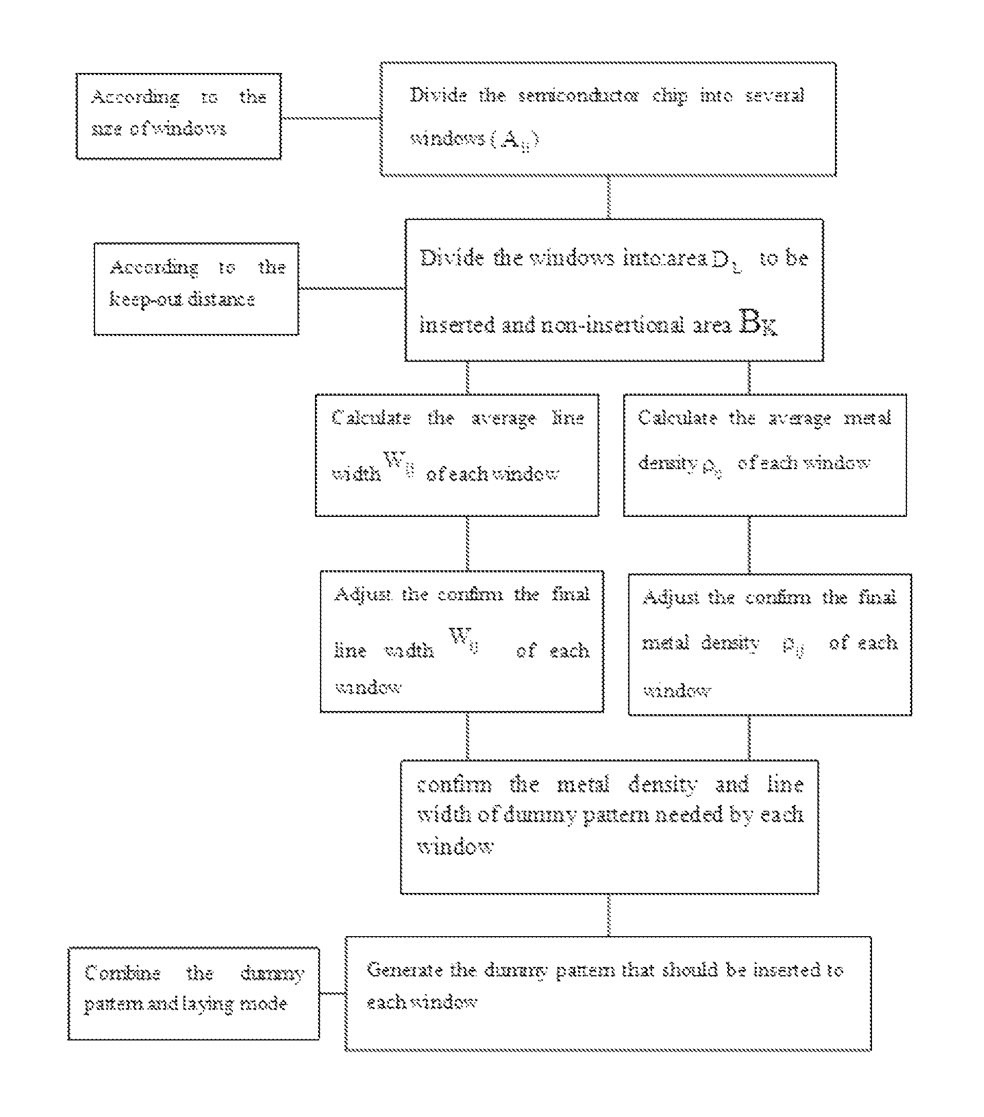
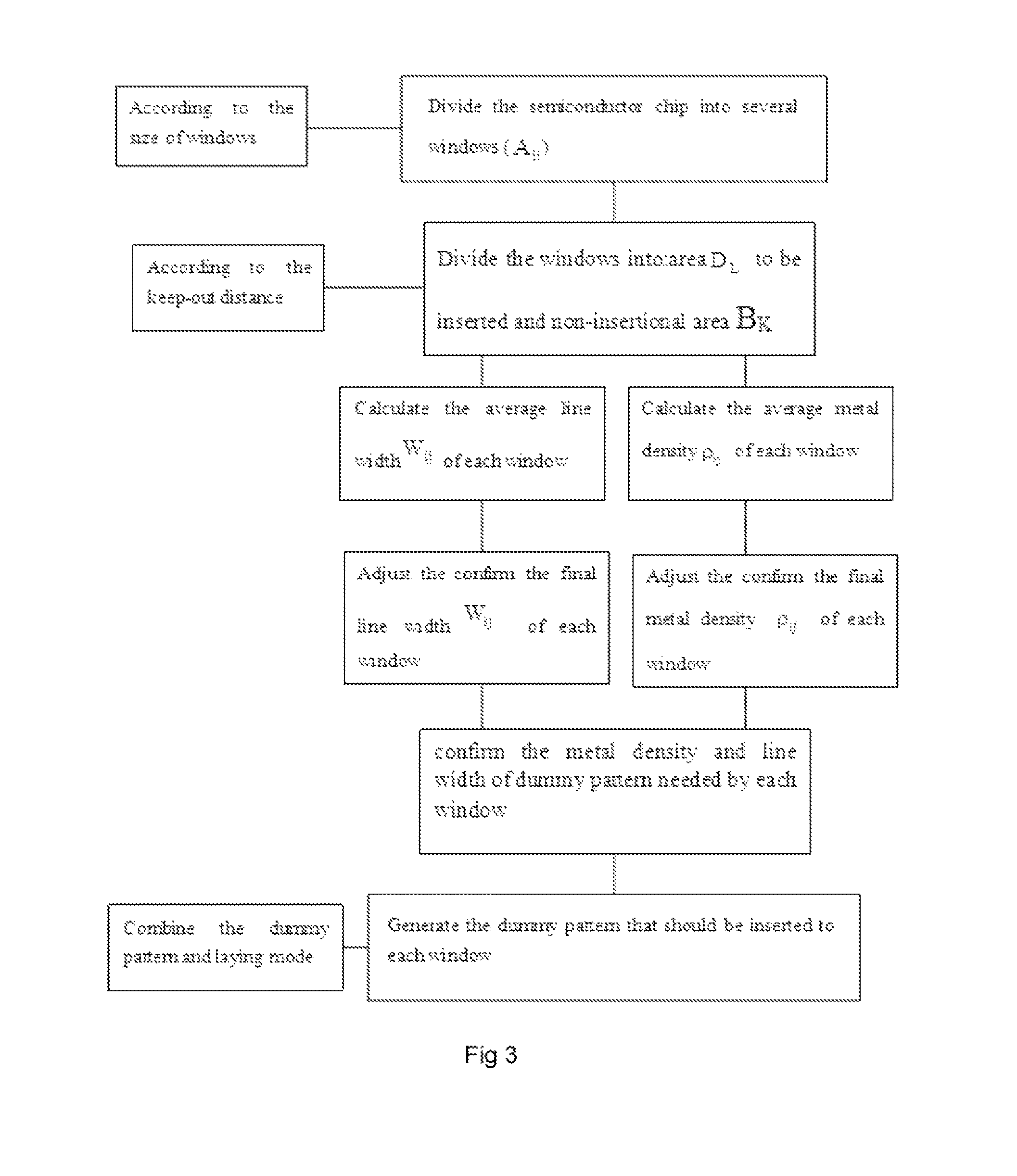
[0046]Illustrated as FIG. 3, the process of the inserting algorithm comprises the following steps:

[0047]Step 1, divide the surface of semiconductor chip into several square windows with an area of A illustrated as FIG. 4, each of which is non-overlapping. Each window is indicated by Aij (the sum of Aij is m*n);

[0048]Step 2, Perform a logic operation on each square window and the window is divided into two parts shown in FIG. 5: the area to-be-inserted which need dummy pattern filling and it is indicated by DL, L is any number from 1 to m the non-inserting area which needn't dummy pattern ...


PUM


Abstract

The present invention disclosed an algorithm of Cu interconnect dummy inserting, including: divide the surface of semiconductor chip into several square windows with an area of A, each of which is non-overlap; perform a logic operation on each square window; and divide the window into two parts: ① the area to-be-inserted; ② the non-inserting area; determine the metal density of the dummy pattern that should be inserted to each square window and the line width; determine the dummy pattern that should be inserted to the windows according to the metal density, line width, the pre-set dummy pattern and the layouting rules. The beneficial effects of the present invention is: avoided the shortcomings of fill density maximization in the rule-based filling method by using reasonable metal density and line width. And with a combination of the influence of line width and density to the copper plating process and chemical mechanical polishing morphology in model-based filling method, it can achieve a better planarization effect.

Description

RELATED APPLICATION[0001]Benefit is claimed under 35 U.S.C 119(a)-(d) to Foreign Application Serial No. 201210049162.5, filed in CHINA, entitled “AN ALGORITHM OF CU INTERCONNECT DUMMY INSERTING” by Shanghai Huali Microelectronics Corporation, filed on Feb. 28, 2012, which is herein incorporated in its entirety by reference for all purposes.TECHNICAL HELD[0002]The present invention is related to the integrated circuit manufacturing technology field, especially an algorithm of Cu interconnect dummy inserting.BACKGROUND[0003]With the continuous development of integrated circuit manufacturing technology and the improvement of the integrated level of the chip, three-dimension and multi-layer configuration is widely used in back-end interconnect. Meanwhile, copper interconnects become the mainstream interconnect technology in the manufacture of integrated circuit because it has lower resistivity, better anti-migration, and it's more conducive to increase device density than aluminum, more...

Claims


Application Information

Patent Timeline
Patent Type & Authority Patents(United States)
IPC IPC(8): G06F17/50
CPCG06F17/5068G06F17/5081G06F2217/12G06F2119/18G06F30/398G06F30/39Y02P90/02
Inventor FANG, JINGXUNCHANG, HSUSHENGFAN, YUNGCHIEH
Owner SHANGHAI HUALI MICROELECTRONICS CORP
Learn More