Low Qgd trench MOSFET integrated with schottky rectifier

a trench mosfet and rectifier technology, applied in the field of integrated circuits, can solve the problems of schottky rectifier, affecting the performance of prior arts, increasing the fabricating cost, etc., and achieves the effects of reducing the specific on-resistance, reducing the forward voltage, and reducing the manufacturing cos

Active Publication Date: 2014-02-18
FORCE MOS TECH CO LTD
View PDF2 Cites 16 Cited by
  • Summary
  • Abstract
  • Description
  • Claims
  • Application Information

AI Technical Summary

Benefits of technology

[0014]One advantage of the present invention is that, a plurality of tilt-angle implanted body dopant region of a second conductivity doping type, e.g. P dopant, marked by p* regions as shown in FIG. 3 to 6, are formed in an N-channel integrated circuit, surrounding lower portions of trenched gates sidewalls to decouple the trenched gates from a drain such that Qgd can be reduced. Furthermore, a plurality of source dopant regions of a first conductivity doping type, e.g. N dopant, marked by n* regions as shown in FIG. 3 to FIG. 6, are formed below trench bottoms of the trenched gates and adjacent to the p* tilt-angle implanted body dopant regions to provide a current path between the drain to a source region such that the p* tilt-angle implanted body dopant regions will not inadvertently increase the resistance between the drain and the source region but Crss can be significantly reduced to a value that is about half or even lower when compared with Crss of prior art because Crss and Qgd will be mainly determined by trench width in the present invention when compared with the prior arts in FIG. 1 and FIG. 2.
[0015]Another advantage of the present invention is that, both the trench MOSFET and the Schottky rectifier are employing trenched contact structure instead of the planar contact structure of prior arts. By employing the trenched contact structure, the integrated circuit is able to shrink to achieve a lower specific on-resistance for the trench MOSFET, and achieve a lower Vf (forward voltage) and lower Ir (reverse leakage current) for the Schottky rectifier.
[0016]Another advantage of the present invention is that, the Schottky rectifier is formed having a Schottky silicide barrier layer along at least trench sidewalls of the trenched contact for the Schottky rectifier, therefore the Schottky rectifier is implemented as trench Schottky rectifier.
[0017]Another advantage of the present invention is that, there is no need to apply an additional body contact region mask for the trench Schottky rectifier in fabricating process, therefore cost saving is achieved.

Problems solved by technology

Both integrated configurations of prior art illustrated in FIG. 1 and FIG. 2 can achieve the integration of the trench MOSFET and the Schottky rectifier on a single semiconductor substrate, however, there are still some disadvantages affecting the performance of prior arts.
Another disadvantage of the prior art is that, the Schottky rectifier is formed by using planar contact structure which occupies a large area, almost one time of the trench MOSFET.
On the other hand, the planar contact structure will lead to a device shrinkage limitation, resulting in high specific on-resistance according to the length dependence of a resistance.
Furthermore, during fabricating process, an additional p+ body contact region mask is required for the Schottky rectifier of prior art, therefore increasing the fabricating cost.

Method used


Image

  • Low Qgd trench MOSFET integrated with schottky rectifier
  • Low Qgd trench MOSFET integrated with schottky rectifier
  • Low Qgd trench MOSFET integrated with schottky rectifier

Examples


Embodiment Construction

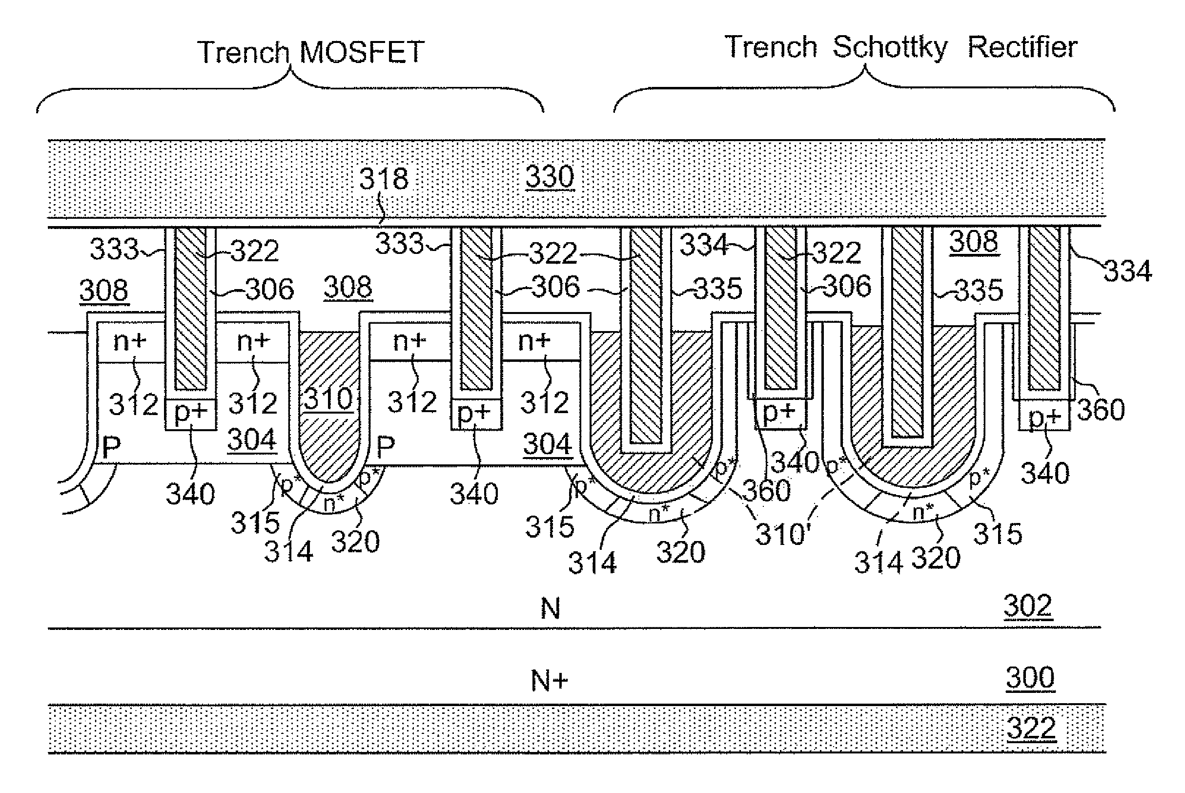
[0030]Please refer to FIG. 3 for a preferred embodiment of the present invention where an N-channel integrated circuit comprising a trench MOSFET and a trench Schottky rectifier is formed on a heavily N+ doped semiconductor substrate 300 with back metal 322 on rear side as a drain. Onto the N+ semiconductor substrate 300, an N epitaxial layer 302 is grown with a same conductivity doping type as the N+ semiconductor substrate 300 and a lower doping concentration. The inventive integrated circuit further comprises a plurality of first type trenched gates 310 for the trench MOSFET and a plurality of second type trenched gates 310′ for the trench Schottky rectifier, wherein the first type trenched gates 310 and the second type trenched gates 310′ are filled with a doped poly-silicon layer padded by a single gate oxide layer 314, wherein the second type trenched gates 310′ have a greater trench width than the first type trenched gates 310. A plurality of P body regions 304 surround trenc...


PUM


Abstract

An integrated circuit includes a plurality of trench MOSFET and a plurality of trench Schottky rectifier. The integrated circuit further comprises: tilt-angle implanted body dopant regions surrounding a lower portion of all trenched gates sidewalls for reducing Qgd; a source dopant region disposed below trench bottoms of all trenched gates for functioning as a current path for preventing a resistance increased caused by the tilt-angle implanted body dopant regions.

Description

CROSS REFERENCE TO RELATED APPLICATIONS[0001]This application is a continuation-in-part (CIP) of U.S. patent application Ser. No. 12 / 385,638, filed on Apr. 15, 2009.BACKGROUND OF THE INVENTION[0002]1. Field of the Invention[0003]This invention relates generally to integrated circuits comprising trench MOSFETs (Metal Oxide Semiconductor Field Effect Transistors) in parallel with trench Schottky rectifiers. More particularly, this invention relates to a novel and improved structure process of fabricating a circuit with integrated trench MOSFETs and trench Schottky rectifiers with a low Qgd (coupling charge between gate and drain).[0004]2. The Prior Arts[0005]The Schottky rectifiers have been used in DC-DC converters. In parallel with a parasitic PN body diode, the Schottky rectifier acts as a clamping diode to prevent the PN body diode from turning on for the reason of higher speed and efficiency, so the recent interests have been focused on the technology to integrate a trench MOSFET...

Claims


Application Information

Patent Timeline
Patent Type & Authority Patents(United States)
IPC IPC(8): H01L29/78
CPCH01L29/4236H01L29/0878H01L29/7806H01L29/872H01L29/8725H01L21/26586H01L29/407H01L29/66734H01L29/456H01L29/1095H01L29/66727H01L29/7813H01L29/41766
Inventor HSIEH, FU-YUAN
Owner FORCE MOS TECH CO LTD
Why Eureka
Try Eureka