Method for eliminating the metal catalyst residues on the surface of wires produced by catalytic growth

a metal catalyst and catalytic growth technology, applied in the field of nanoscale wires, can solve the problems of metal catalyst residues on the surface of wires, metal catalyst residues are harmful in respect of a large number of applications, and significant deterioration in the performance of devices

Inactive Publication Date: 2014-03-11
COMMISSARIAT A LENERGIE ATOMIQUE ET AUX ENERGIES ALTERNATIVES
View PDF1 Cites 58 Cited by
  • Summary
  • Abstract
  • Description
  • Claims
  • Application Information

AI Technical Summary

Benefits of technology

[0044]In an intermediate step, i.e. after the step of the catalytic growth of the solid structures made from a first material, it is possible to implement an initial at least partial elimination of the catalyst, and to advantage by etching. In this step and as already described elsewhere, it is possible to eliminate at least partially the catalyst which has been drawn to the free end of the solid structure.

Problems solved by technology

Furthermore, when growing wires catalytically, metal catalyst residues may remain on the surface of the wires.
In fact, metal catalyst residues are harmful in respect of a large number of applications.
For example, for silicon wires intended for uses in electronics or photovoltaics, the presence of metals such as gold or copper brings about significant deterioration in the performance of the devices, as these metals cause the appearance of deep electronic traps in the forbidden band of silicon.
However, eliminating metal catalyst residues by etching the metal is often of limited effectiveness.
In particular, for wires comprising materials that are air oxidizable, as is the case with silicon, metal etching may become ineffectual through the formation, on the surface of the wire, of a layer of oxide.

Method used


Image

  • Method for eliminating the metal catalyst residues on the surface of wires produced by catalytic growth
  • Method for eliminating the metal catalyst residues on the surface of wires produced by catalytic growth
  • Method for eliminating the metal catalyst residues on the surface of wires produced by catalytic growth

Examples


example 1

2. Example 1

Step 1: Growing Silicon Nanowires

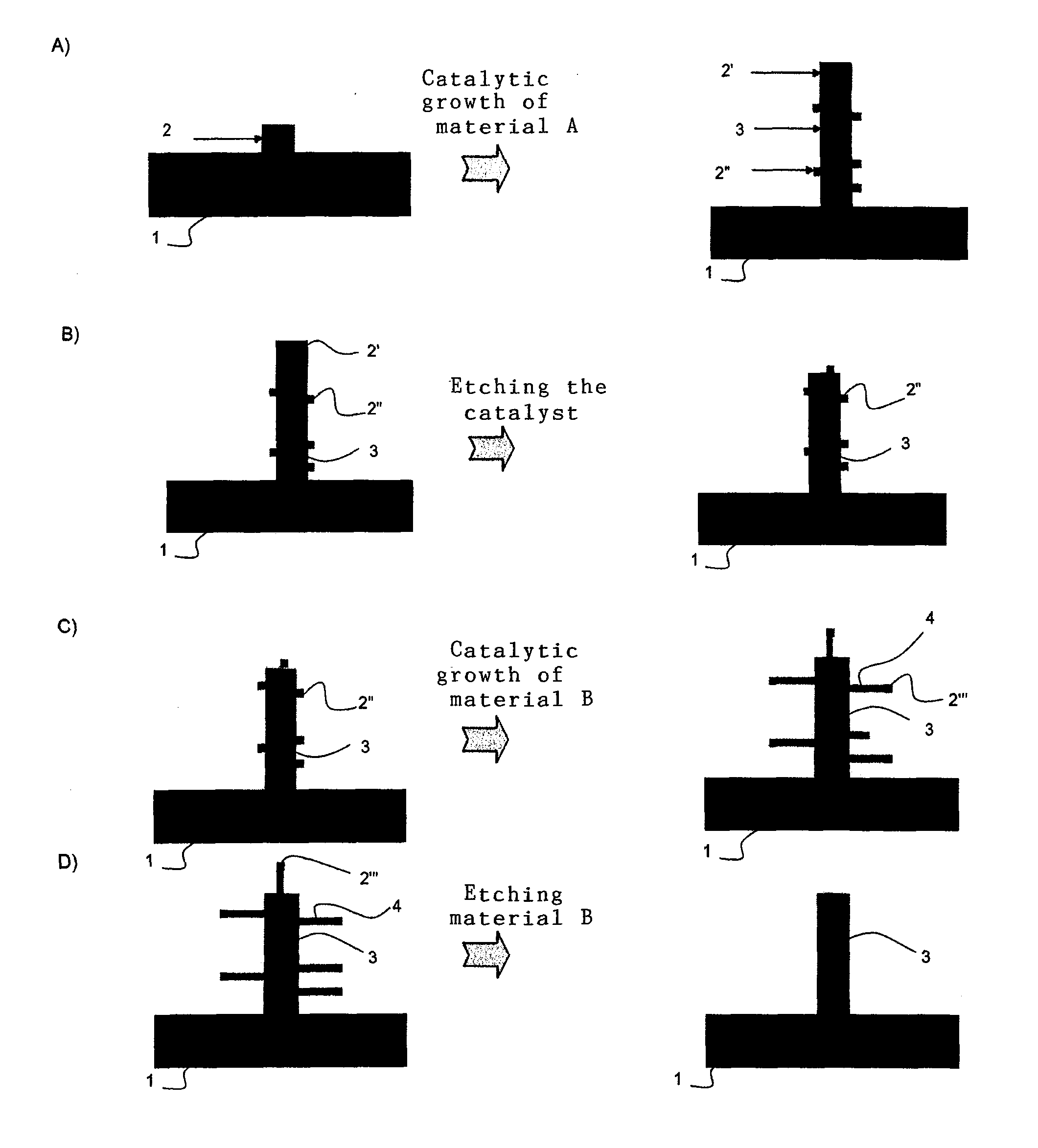
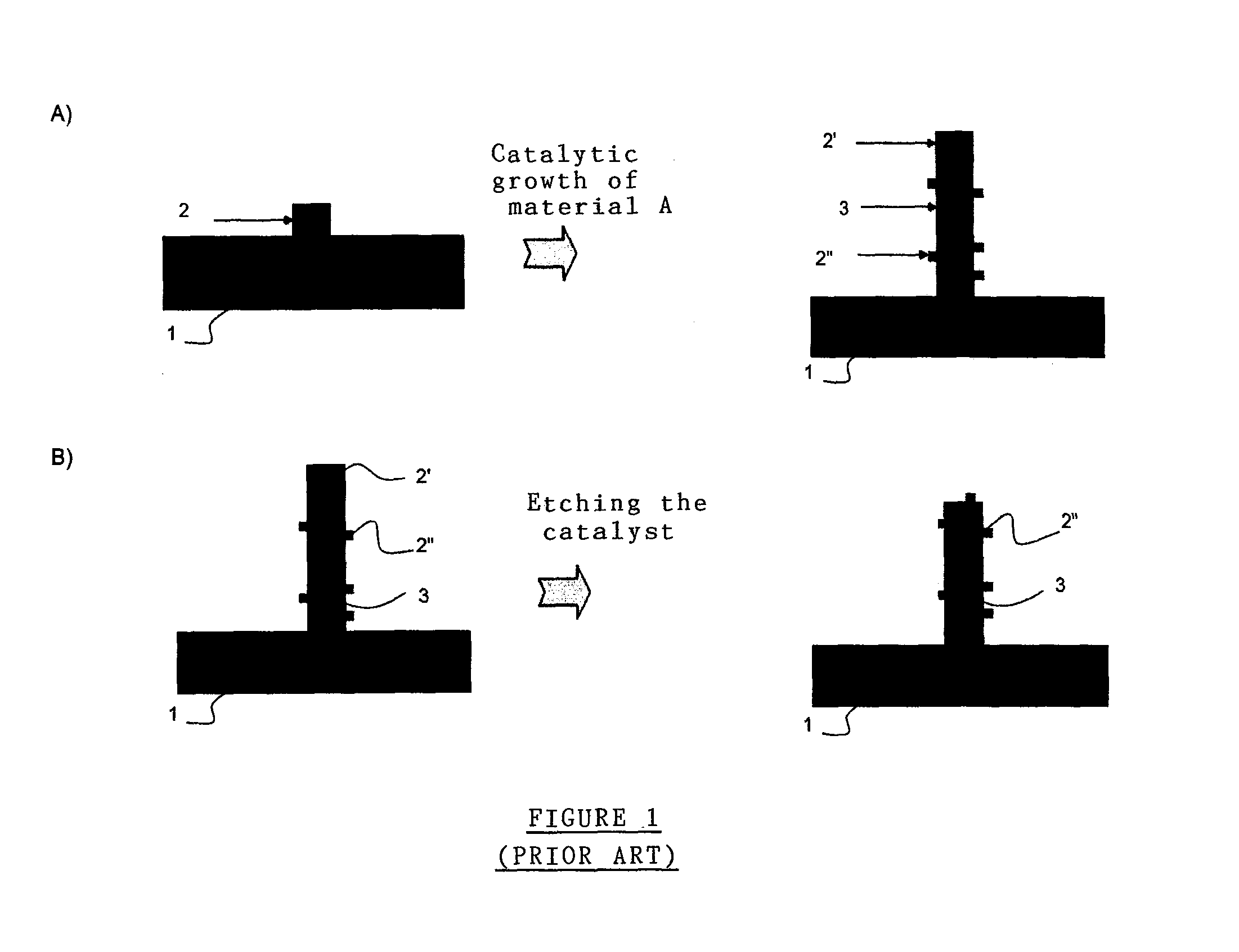
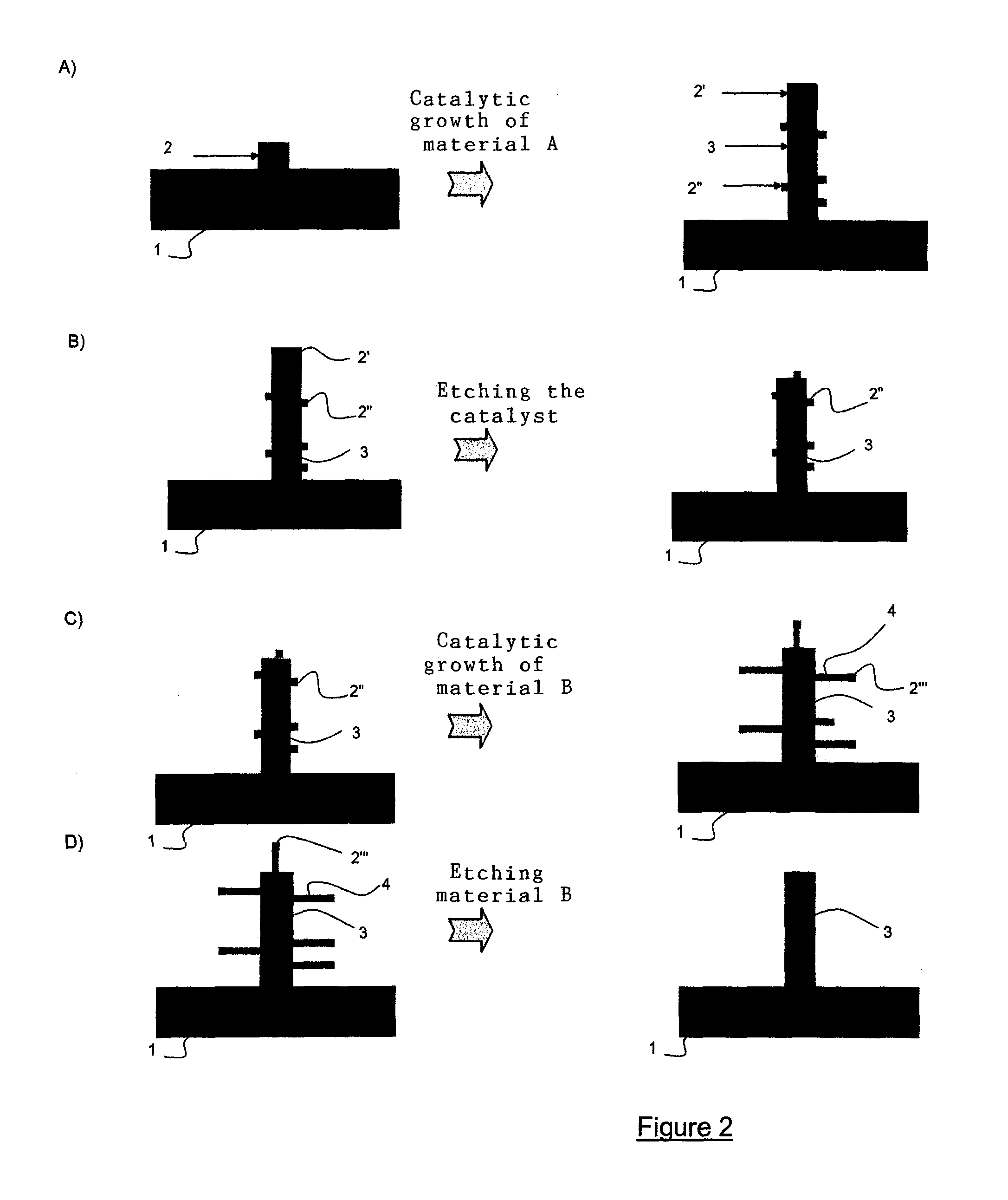
[0062]The main wire (3) is a silicon wire (Si=material A) 100 nanometers in diameter, developed using a metal catalyst of gold (2).

[0063]The operating conditions are as follows:[0064]colloidal gold nanoparticles (100 nm) on Si (111) substrate;[0065]T=650° C.;[0066]P=10 mbar;[0067]mix SiH4 (silane)+H2 (hydrogen);[0068]duration: 20 nm.

Step 2: Gold Etching

[0069]solution marketed under the reference “IKI2” by the Company VWR Prolabo, constituted by an aqueous solution of KI (potassium iodide) and iodine I2, at ambient temperature;[0070]duration: 10 nm.

Step 3: Growing Silicon-Germanium Nanowires

[0071]Catalytic growth of sacrificial wires (4) made of silicon-germanium. (Si1-xGex with x=0.4), from gold residues (2″) present on the surface of the main wire (3).

[0072]Operating conditions as follows:[0073]T=550° C.;[0074]P=10 mbar;[0075]mix SiH4 (silane)+GeH4 (germane)+H2 (hydrogen), with ratio [GeH4 flux / SiH4 flux]=1.5;[0076]duration 10 nm.

Step 4:...

example 2

3. Example 2

Step 1: Growing Nanowires of GaAs

[0081]The main wire (3) is a wire of gallium arsenide (GaAs=material A) 100 nm in diameter, developed using a metal catalyst of gold (2).

[0082]Operating conditions:[0083]colloidal gold nanoparticles (100 nm) on GaAs (111) substrate;[0084]T=450° C.;[0085]P=100 mbar;[0086]mix TMGa (trimethylgallium)+AsH3 (arsine);[0087]duration: 20 nm.

Step 2: Gold Etching

[0088]solution marketed under the reference “IKI2” by the Company VWR Prolabo, constituted by an aqueous solution of KI (potassium iodide) and iodine I2, at ambient temperature;[0089]duration: 10 nm.

Step 3: Growing Nanowires of InAs

[0090]Catalytic growth of sacrificial wires (4) of indium arsenide (InAs), from gold residues (2″) present on the surface of the main wire (3).

[0091]Operating conditions as follows:[0092]T=450° C.;[0093]P=100 mbar;[0094]mix TMIn (trimethylindium)+AsH3 (arsine);[0095]duration 10 nm.

Step 4: Etching Nanowires of InAs

[0096]Selective etching of the indium arsenide (=m...


PUM


Abstract

A method is provided for eliminating catalyst residues that are present on the surface of solid structures. The solid structures are made from a first material and are obtained by catalytic growth from a substrate. The method includes the following steps: catalytically growing, from the catalyst residues, solid structures made from a second material; and selectively eliminating the solid structures made from the second material, thereby eliminating the catalyst residues.

Description

CROSS REFERENCE TO RELATED APPLICATION[0001]This application claims priority to French Patent Application No. 1057595 filed on Sep. 22, 2010.FIELD OF INVENTION[0002]This invention concerns a method for eliminating the traces of catalyst residues present on the surface of solid structures, and in particular nanoscale wires, obtained by catalytic growth.[0003]This method is of particular advantage in the field of electronics or photovoltaics, where the presence of residual catalyst brings about significant deterioration in the performance of the devices involved.BACKGROUND OF THE INVENTION[0004]Solid structures in the form of wires, with a diameter of between a few nanometers and a few millimeters, may be developed by catalytic growth.[0005]The Kolasinski document (Current Opinion in Solid State and Materials Science 10, 182-191 (2006)) describes various alternatives of this technology particularly in relation to:[0006]catalytic growth mechanisms: vapor-liquid-solid, vapor-solid-solid...

Claims


Application Information

Patent Timeline
Patent Type & Authority Patents(United States)
IPC IPC(8): H01L21/20H01L21/36
CPCH01L29/0676B82Y40/00H01L21/02645H01L21/02521H01L21/02546H01L21/02532H01L21/0245H01L21/02463H01L21/02664H01L21/02603B82B3/00B82B1/00
Inventor PERRAUD, SIMONCORONEL, PHILIPPE
Owner COMMISSARIAT A LENERGIE ATOMIQUE ET AUX ENERGIES ALTERNATIVES
Why Eureka
Try Eureka