Check patentability & draft patents in minutes with Patsnap Eureka AI!

Electro-optical device and driving circuit

a technology of optical devices and driving circuits, applied in the field of optical devices, can solve the problems of power consumption, power may vary, and the voltage of the capacitance line may not reach the desired voltage level quickly, so as to prevent the deterioration of display quality and reduce the noise

Active Publication Date: 2014-03-11
JAPAN DISPLAY WEST
View PDF17 Cites 1 Cited by
  • Summary
  • Abstract
  • Description
  • Claims
  • Application Information

AI Technical Summary

Benefits of technology

This configuration prevents system shutdowns by ensuring consistent voltage application across the capacitance line, reducing power consumption, and maintaining display quality by avoiding high impedance states and noise effects.

Problems solved by technology

When an AC drive of the pixel capacitances is required, voltage of a data signal fluctuates between both polarities and therefore elements of a data-line-driving circuit supplying data signals to a data line need to have a resistance characteristic against the voltage amplitude, which is disadvantageous for power-consumption point of view.
When a capacitance-line-driving circuit is provided at one side of the capacitance line, a delay occurs at the other side of the capacitance line and voltage of the capacitance line may not reach a desired voltage level rapidly.
However, when the capacitance-line-driving circuits are provided on both sides of the capacitance line, since output conditions of latch circuits provided at both sides of the capacitance line have not been settled yet, output conditions of the latch circuit immediately after applying power may be different from each other.
If the output conditions are different from each other, the whole system may shutdown immediately after applying power, because a high voltage value of the two-value voltage and a low voltage value of the two-value voltage are applied to one side and the other side of the capacitance line respectively, causing a very large current to flow.

Method used


Image

  • Electro-optical device and driving circuit
  • Electro-optical device and driving circuit
  • Electro-optical device and driving circuit

Examples


first embodiment

[0023

[0024]Above all, a first embodiment of the invention will be described. FIG. 1 is a block diagram showing a configuration of an electro-optical device according to the first embodiment.

[0025]As shown in FIG. 1, an electro-optical device 10 is peripheral-circuit-containing panel including a display area 100, and around the display area 100, a scanning-line-driving circuit 140, a capacitance-line-driving circuits 150L and 150R, and a data-line-driving circuit 190. Further, a display-control circuit 20 is connected to the peripheral-circuit-containing panel by, for example, a flexible printed circuit (FPC) board.

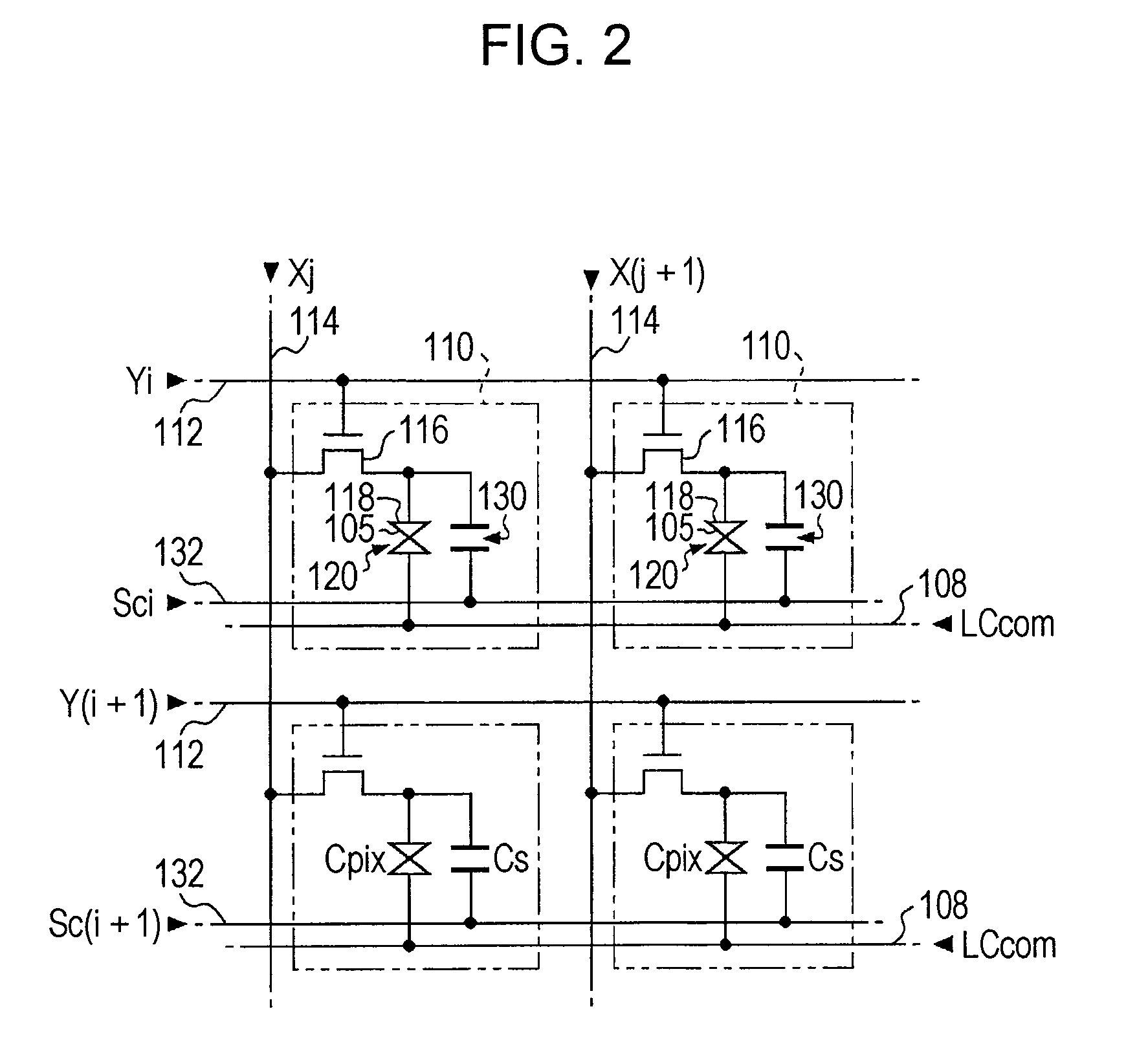
[0026]The display area 100 is an area in which pixels 110 are arranged, and in the embodiment, while scanning lines 112 of total 322 rows from row 0 to row 321 extends in the row direction in the figure, data lines 114 of 240 columns extends in the column direction.

[0027]In FIG. 1, respective pixels 110 are arranged corresponding to the intersections between the data lines...

second embodiment

[0056

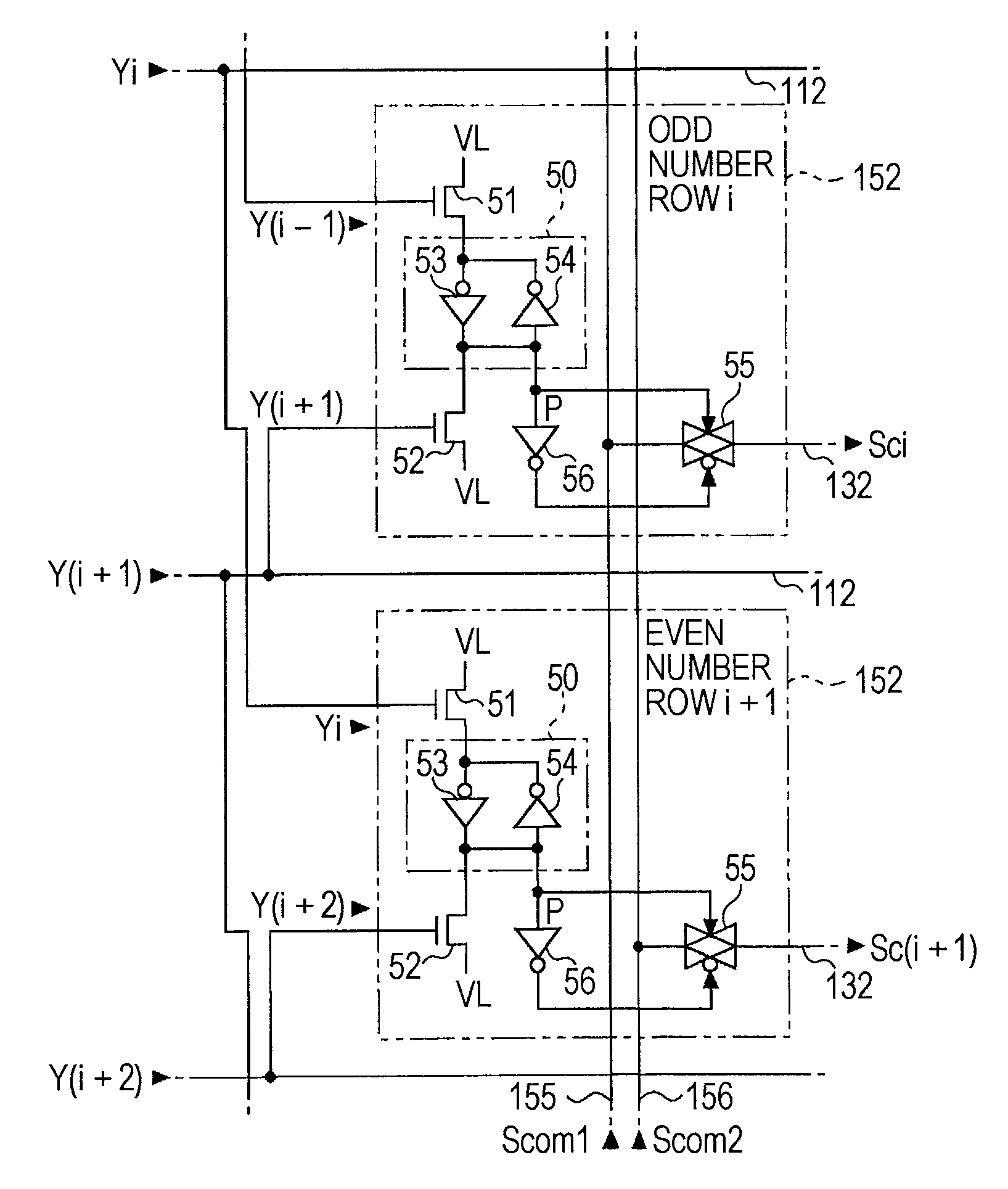
[0057]Next, an electro-optical device according to a second embodiment will be described. FIG. 7 is a block diagram showing a configuration of the electro-optical device according to the second embodiment. In the first embodiment shown in FIG. 1, while a writing polarity is inverted by one row at a time, in the second embodiment, the writing polarity is inverted by two rows at a time. Therefore, the second embodiment is different from the first embodiment in terms of two points: one is that the capacitance signal of the second embodiment includes a first capacitance signal Scom1 and a second capacitance signal Scom2 (a first difference), and the other is that in the capacitance-line-driving circuits 150L and 150R the connection relation of the unit control circuits 152 in odd-numbered rows is different from that in even-numbered rows (a second difference). Since the second embodiment has similar configurations to the first embodiment other than the above differences, the follow...

third embodiment

[0065

[0066]In the first and the second embodiment described above, for example as for a row i, the terminal P in the unit control circuit 152 is maintained at L level except two horizontal-scanning periods including horizontal-effective-scanning periods in which the row i and row i−1 are selected. On this account, except the two horizontal-scanning periods, the transmission gate 55 becomes an off-state, and therefore the capacitance line 132 is not connected to any signal line 153 (155 and 156) (high impedance state), and the voltage of the capacitance line 132 is maintained only by the parasitic capacitance or the like. Under such high impedance state, if noise or the like are superposed on the capacitance line 132, voltage of the capacitance line 132 is varied from the voltages VSH and VSL. The voltage variation of the capacitance line 132 effects on the sustaining voltage of the pixel capacitances 120 of one row which share the capacitance line 132, causing deterioration of the d...


PUM


Abstract

A driving circuit of an electro-optical device, a capacitance-line-driving circuit shifting voltage of a capacitance line to one voltage of two-value voltage, and the capacitance-line-driving circuit includes a unit control circuit provided correspondingly to the capacitance line at both end portions of the capacitance line, and the unit control circuit corresponding to one capacitance line includes, a latch circuit maintaining a logic level at one level for at least a period of the scanning line corresponding to the one capacitance line being selected, a switch provided between the capacitance line and a signal line supplying a capacitance signal in which the two-value voltage is switched over at a predetermined cycle, the switch being electrically connected when the logic level is one level and electrically disconnected when the logic level is the other level.

Description

BACKGROUND[0001]1. Technical Field[0002]The present invention relates to an electro-optical device such as a device using liquid crystal or the like, in which a voltage amplitude of a data line is suppressed.[0003]2. Related Art[0004]In an electro-optical device such as a device using liquid crystal or the like, a pixel capacitance (liquid crystal capacitance) is provided at intersections between scanning lines and data lines. When an AC drive of the pixel capacitances is required, voltage of a data signal fluctuates between both polarities and therefore elements of a data-line-driving circuit supplying data signals to a data line need to have a resistance characteristic against the voltage amplitude, which is disadvantageous for power-consumption point of view. In order to suppress the voltage amplitude of a data line, there has been proposed technology in which an auxiliary capacitance is provided parallel to pixel capacitance and a capacitance line is driven with a two-value volt...

Claims


Application Information

Patent Timeline
Patent Type & Authority Patents(United States)
IPC IPC(8): G09G5/00
CPCG09G2300/043G09G2310/0262G09G3/3648G09G2330/021G09G2300/0876G09G3/3614G09G2300/0426
Inventor FUJITA, SHIN
Owner JAPAN DISPLAY WEST
Features
  • R&D
  • Intellectual Property
  • Life Sciences
  • Materials
  • Tech Scout
  • Unparalleled Data Quality
  • Higher Quality Content
  • 60% Fewer Hallucinations
Learn More