Bit line voltage bias for low power memory design

a low-power memory and bit line voltage bias technology, applied in static storage, information storage, digital storage, etc., can solve the problems of consuming power, affecting the maximum operational speed, so as to reduce the current inrush

Inactive Publication Date: 2014-03-18
TAIWAN SEMICON MFG CO LTD
View PDF5 Cites 9 Cited by
  • Summary
  • Abstract
  • Description
  • Claims
  • Application Information

AI Technical Summary

Benefits of technology

[0013]Among other advantages, the respective embodiments facilitate switching quickly from the sleep mode to the standby mode upon transition of the SLP signal (and optionally also a complementary SLPB signal). In preparation for a read operation, for example, the transition in SLP / SLPB is accompanied by a transition in the bit line precharge signal BLEQ, for bringing both bit lines BL, BLB up to the supply voltage VDD. However, the change to standby mode is not accompanied by as large a rush of current at either BL or BLB as would occur in the absence of bit line bias control, because the bit line bias control configuration has maintained the bit line voltages near the positive supply voltage, namely at VDD less difference voltage ΔV.
[0015]Advantageously, a connecting transistor is coupled between the bit lines of the complementary pair and is responsive to the control signal for coupling the bit lines to one another when in the sleep mode. The effect is to bring the floating bit lines to equal voltages substantially at the supply voltage less a difference voltage ΔV. The difference voltage is less than the difference between logic states. Preliminarily fixing the floating bit line voltages at the supply voltage less ΔV, reduces the inrush of current that could be experienced at one or more bit positions when switching into the standby-ready mode.

Problems solved by technology

Where a potential difference exists across the source / drain or gate / substrate of the transistors of the inverters or passing gates, some current leakage occurs.
Isolating the nodes of the bit cell at the inputs / outputs of the cross coupled inverters, and also allowing the bit lines to float until a bit cell position is addressed, reduces but does not eliminate current leakage.
These restoration steps when switching from the sleep mode to the ready or standby mode and preparing for a memory access operation, take time that can adversely affect the maximum operational speed.
Restoration steps also consume power, and require that the power supply and its conductors have sufficiently high capacity and sufficiently low IR voltage drops, to handle the increased loading associated with switching into the standby-ready mode.

Method used


Image

  • Bit line voltage bias for low power memory design
  • Bit line voltage bias for low power memory design
  • Bit line voltage bias for low power memory design

Examples


Embodiment Construction

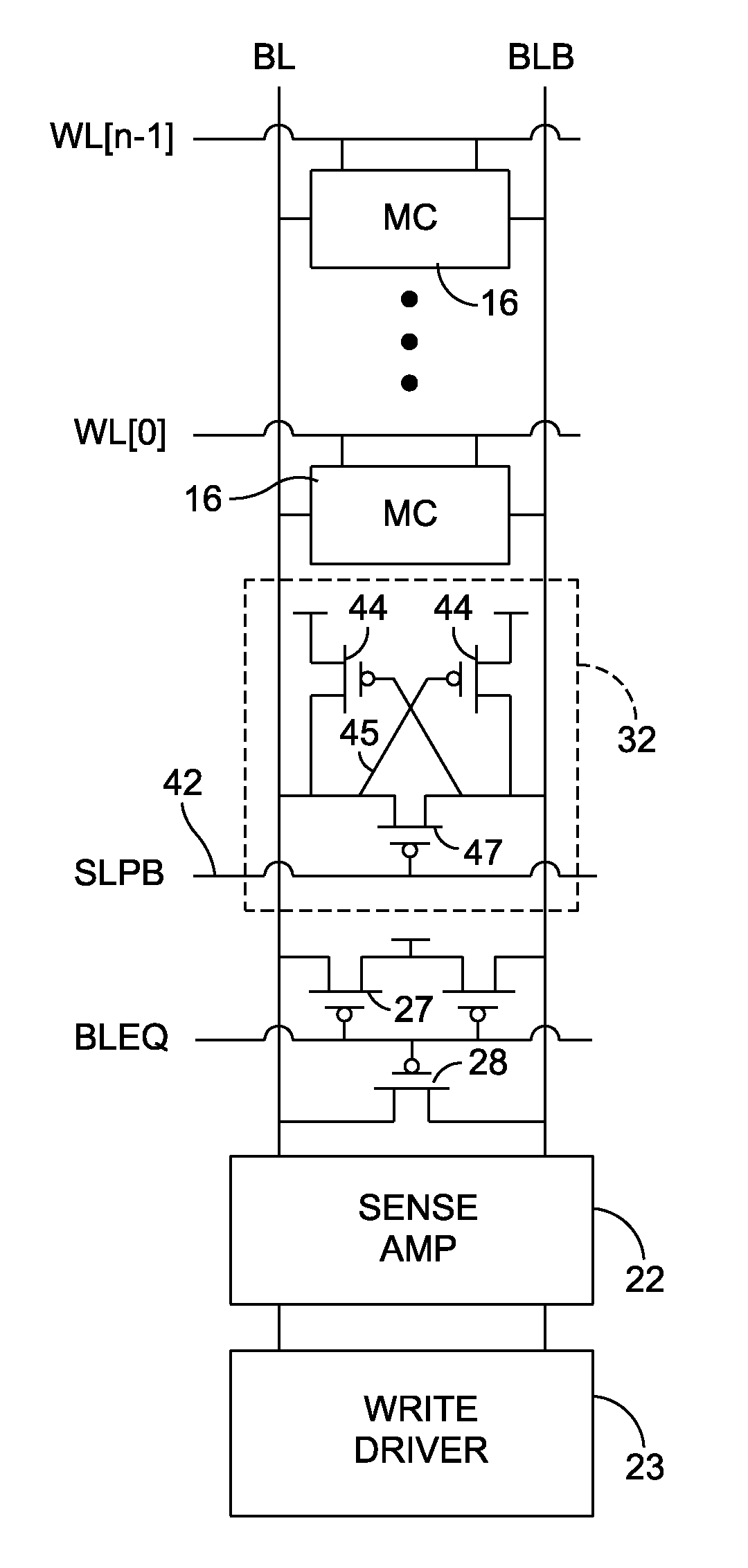
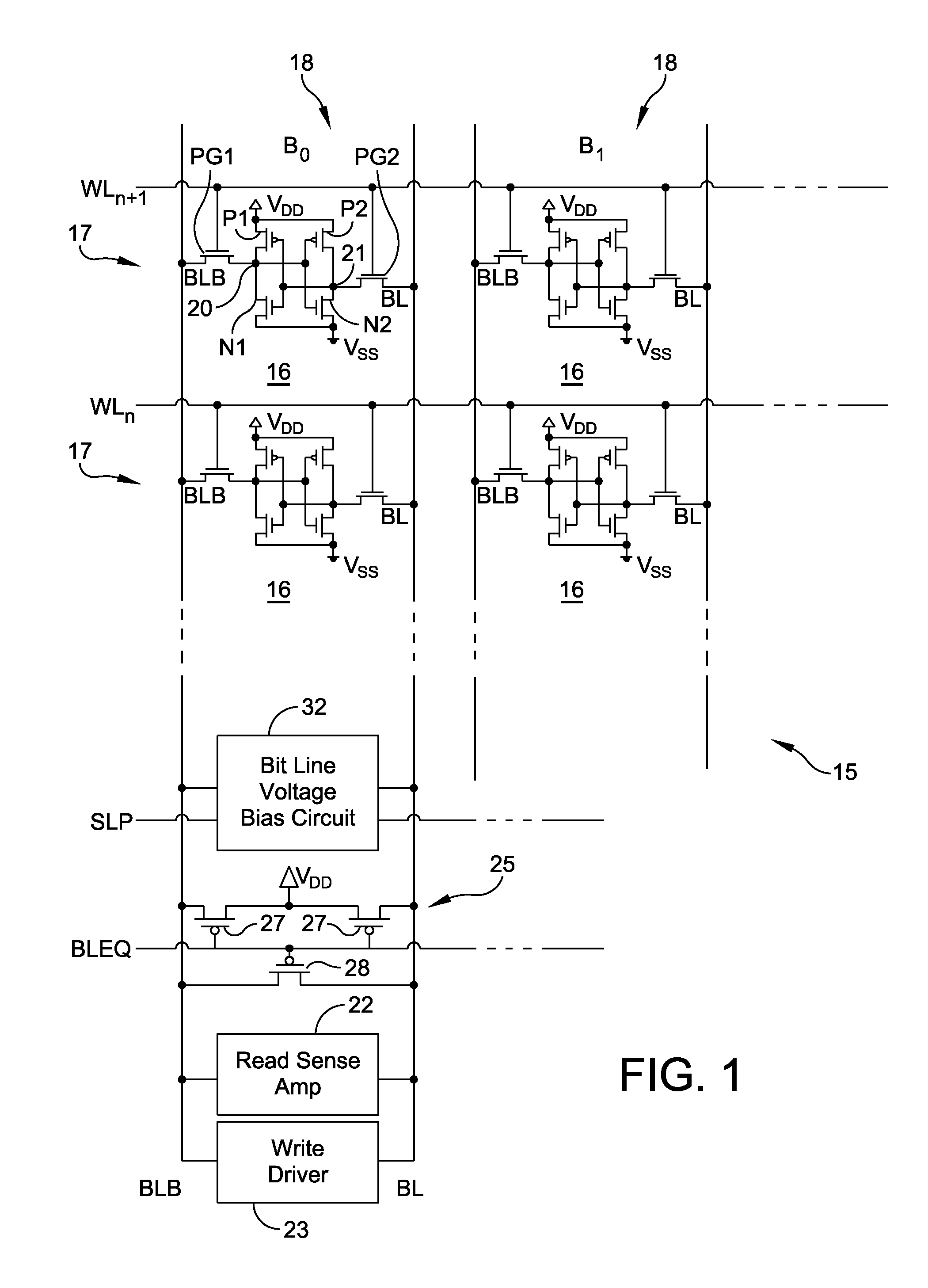
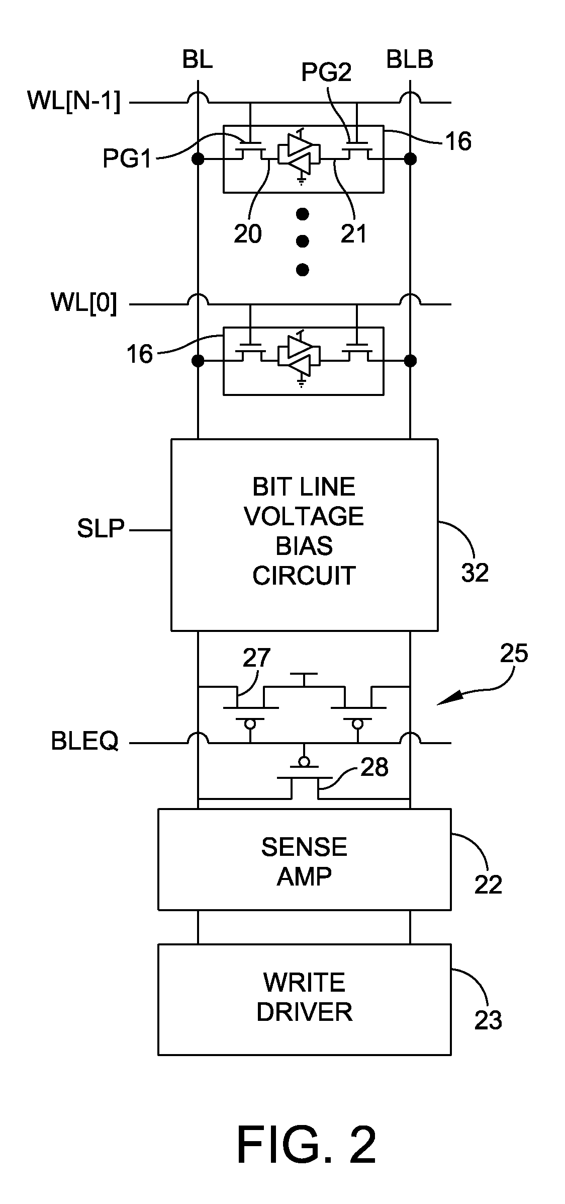
[0027]In FIG. 1, a six-transistor (6T) bit cell in a CMOS SRAM (complementary metal oxide semiconductor static random access memory) 15 is shown as an example of an integrated circuit memory device that stores one bit per bit cell 16. Numerous bit cells are provided in a memory array shown with rows or words 17 and columns or bit positions 18 in the words. A row 17 of bit cells 16 is selected by activating a word line signal WL for that row. The logic levels of the bit cells 16 in the row 17 are loaded (written) or sensed (read) by signals on bit lines BL and BLB that cross the word line at each selected bit cell position in the array.

[0028]The cells 16 have four transistors forming two cross coupled inverters, each inverter having a PMOS transistor and an NMOS transistor coupled to one another at a node, and the inverter connected between positive and negative power supplies VDD, VSS. The cell nodes 20, 21 are isolated from the complementary bit lines BL and BLB by passing gate swi...


PUM


Abstract

In a digital memory with an array of bit cells coupled to word lines and bit lines, each bit cell having cross coupled inverters isolated from bit lines by passing gate transistors until addressed, some or all of the bit cells are switchable between a sleep mode and a standby mode in response to a control signal. A bit line bias circuit controls the voltage at which the bit lines are caused to float when in the sleep mode. A pull-up transistor for each bit line BL or BLB in a complementary pair has a conductive channel coupled to a positive supply voltage and a gate coupled to the other bit line in the pair, BLB or BL, respectively. A connecting transistor also can be coupled between the bit lines of the complementary pair, bringing the floating bit lines to the supply voltage less a difference voltage ΔV.

Description

BACKGROUND[0001]This disclosure relates to the field of static random access memories and similar circuits that maintain stored logic levels while power is applied, in particular with provisions to reduce power consumption when in an inactive or “sleep” mode. Bit lines are biased in sleep mode according to several embodiments, so as to facilitate switching into a standby mode for read or write operations, without an undue inrush of current to power up.[0002]So long as power is applied to a volatile memory bit cell, the logic level of the bit cell is stable. Typically, two cross-coupled inverters hold one another in a present logic state that can be read out using a sense amplifier. The inverters can be forced by a write driver to switch to an opposite logic state, and then remain stable in that logic state. A sense amplifier and a driver are provided at each bit position in a bit cell array having plural word lines. For example, an array might have 256 bit positions and 256 word lin...

Claims


Application Information

Patent Timeline
Patent Type & Authority Patents(United States)
IPC IPC(8): G11C5/14
CPCG11C7/12G11C11/419
Inventor CHENG, HONG-CHENYANG, JUNG-PINGCHENG, CHITINGLEE, CHENG-HUNGDONG, SANG H.LIAO, HUNG-JEN
Owner TAIWAN SEMICON MFG CO LTD
Why Eureka
Try Eureka