

Film for flip chip type semiconductor back surface
a semiconductor back surface and flip chip technology, applied in the field of film for flip chip type semiconductor back surface, can solve the problems of semiconductor chip damage, increase in the number of steps, increase in cost and the like, etc., and achieve excellent laser marking property, excellent appearance property, excellent holding force
- Summary
- Abstract
- Description
- Claims
- Application Information
AI Technical Summary
Benefits of technology
Problems solved by technology
Method used
Image

Examples
production example 1
[0221]21 parts of an epoxy resin (a trade name “EPICOAT 1004” manufactured by JER Co., Ltd.), 22 parts of a phenol resin (a trade name “MILEX XLC-4L” manufactured by Mitsui Chemicals, Inc.), and 77 parts of sphere silica (a trade name “SO-25R” manufactured by Admatechs Co., Ltd., average particle diameter: 0.5 μm) based on 100 parts of an acrylic acid ester-based polymer (a trade name “PARACRON W-197CM” manufactured by Negami Chemical Industrial Co., Ltd.) having ethyl acrylate and methyl methacrylate as main components were dissolved into methyl ethyl ketone to prepare a resin composition solution having a solid concentration of 23.6% by weight (sometimes referred to as “resin composition solution A”).
production example 2
[0222]113 parts of an epoxy resin (a trade name “EPICOAT 1004” manufactured by JER Co., Ltd.), 121 parts of a phenol resin (a trade name “MILEX XLC-4L” manufactured by Mitsui Chemicals, Inc.), 246 parts of sphere silica (a trade name “SO-25R” manufactured by Admatechs Co., Ltd., average particle diameter: 0.5 μm), 5 parts of a dye 1 (a trade name “OIL GREEN 502” manufactured by Orient Chemical Industries Co., Ltd.), and 5 parts of a dye 2 (a trade name “OIL BLACK BS” manufactured by Orient Chemical Industries Co., Ltd.) based on 100 parts of an acrylic acid ester-based polymer (a trade name “PARACRON W-197CM” manufactured by Negami Chemical Industrial Co., Ltd.) having ethyl acrylate and methyl methacrylate as main components were dissolved into methyl ethyl ketone to prepare a resin composition solution having a solid concentration of 23.6% by weight (sometimes referred to as “resin composition solution B”).
(Evaluation of Adhesiveness to Wafer)
[0223]With regard to the resin layers ...
example 1
Manufacture of Film for Semiconductor Back Surface
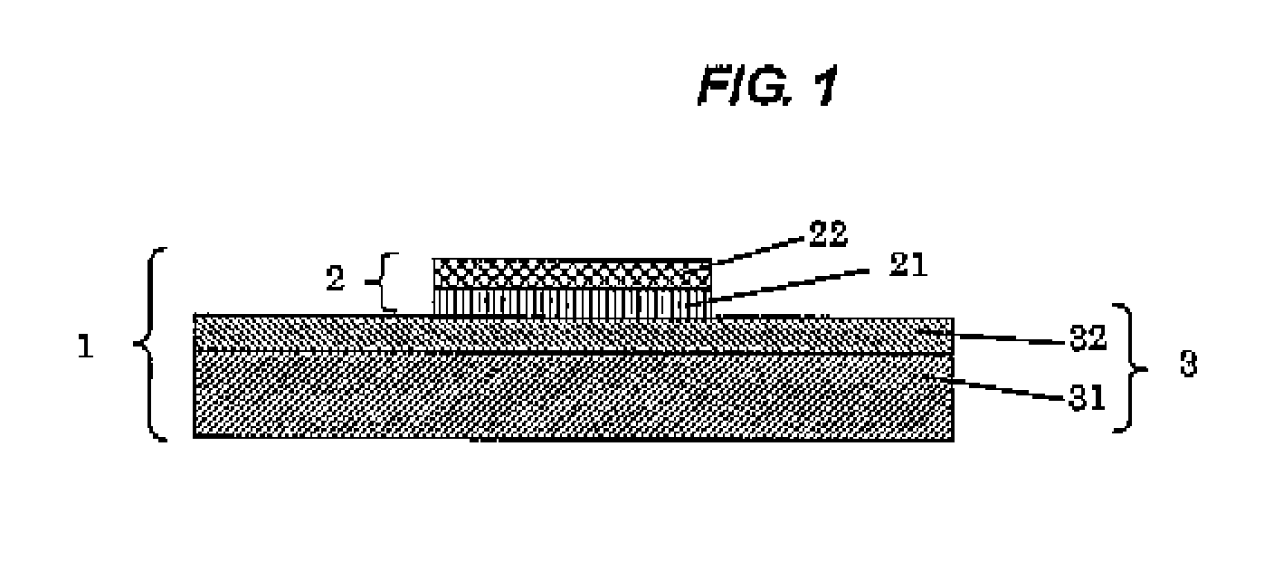
[0239]The resin composition solution A prepared in Production Example 1 was applied onto a releasably treated film as a release liner (separator) composed of a polyethylene terephthalate film having a thickness of 50 μm, which had been subjected to a silicone-releasing treatment, and then dried at 130° C. for 2 minutes to form a wafer-side resin layer (wafer adhesion layer) having a thickness (average thickness) of 10 μm. Thereafter, the resin composition solution B prepared in Production Example 2 was applied onto the wafer-side resin layer (wafer adhesion layer) and then dried at 130° C. for 2 minutes to form an outer resin layer (laser marking layer) having a thickness (average thickness) of 10 μm, thereby manufacturing a film for semiconductor back surface (sometimes referred to as “film A for semiconductor back surface”) having a thickness (average thickness) of 20 μm
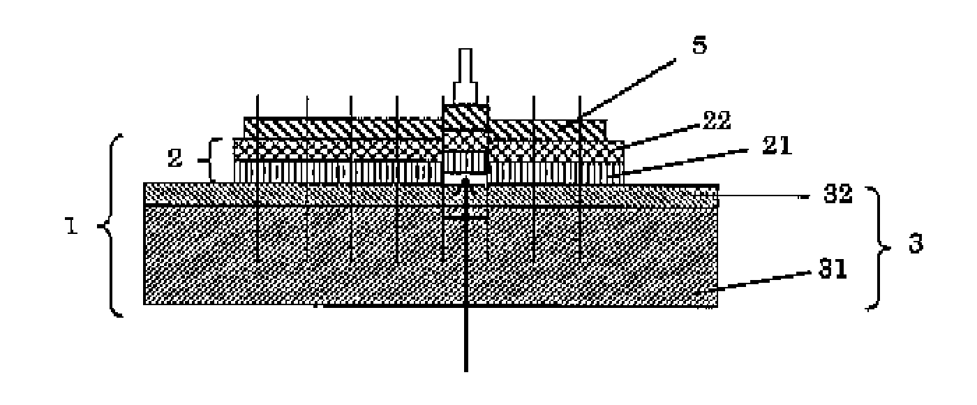
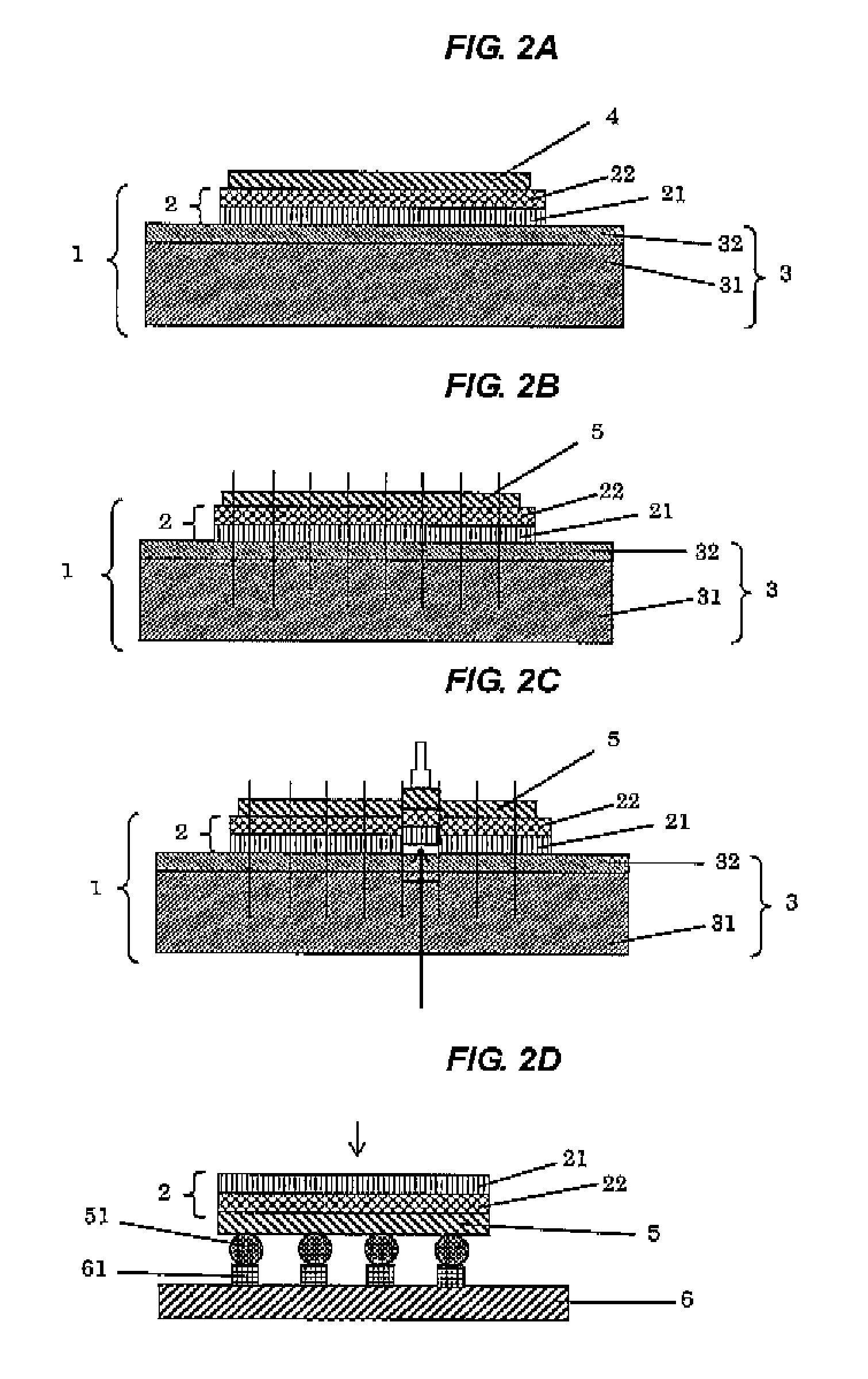
[0240]The above film A for semiconductor back surface was atta...
PUM
| Property | Measurement | Unit |
|---|---|---|
| light transmittance | aaaaa | aaaaa |
| thickness | aaaaa | aaaaa |
| wavelength | aaaaa | aaaaa |
Abstract
Description
Claims
Application Information