Method of manufacturing nitride semiconductor and nitride semiconductor element

a manufacturing method and technology of nitride semiconductor, applied in the direction of polycrystalline material growth, crystal growth process, chemically reactive gas, etc., can solve the problems of difficult fabrication of nitride semiconductor in bulk single crystal form, unfavorable surface morphology, and myriad irregularities in the gan semiconductor layer, so as to prevent thermal distortion of the aln buffer layer by the difference in growth temperature, prevent the degradation of the aln buffer layer by heating, and prevent the effect of unfavor

Active Publication Date: 2014-04-29
ROHM CO LTD
View PDF19 Cites 149 Cited by
  • Summary
  • Abstract
  • Description
  • Claims
  • Application Information

AI Technical Summary

Benefits of technology

[0023]According to the present invention, after the supply of the Al (aluminum)-source material of the AlN buffer layer to be formed at a growth temperature of 900° C. or higher is started, the supply of the N (nitrogen)-source material is started. The supply of the N (nitrogen)-source material is carried out intermittently (on-and-off). Accordingly, while the mole ratio of the N-source material / Al-source material is set to be a relatively high value so that Al is prevented from being taken in the crystallinity of the nitride semiconductor crystal, the nitride semiconductor crystal can be formed with a favorable surface morphology.
[0024]In addition, the AlN buffer layer is formed at a high temperature of 900° C. or higher. Accordingly, the temperature at the formation of the AlN buffer layer scarcely differs from the temperature for growing the nitride semiconductor crystal the layer of which is to be formed on top of the buffer layer. The growth of the nitride semiconductor crystal can be started quickly, and the degradation of the AlN buffer layer by the heating can be prevented. In addition, the thermal distortion of the AlN buffer layer by the difference in the growth temperature can be prevented.

Problems solved by technology

The manufacturing of nitride semiconductor in a form of bulk single crystal is difficult.
However, the GaN semiconductor layer that is grown directly on top of the sapphire substrate by the MOCVD method has a hexagonal pyramid growth pattern or a hexagonal column growth pattern, so that the surface of the GaN semiconductor layer has a myriad of irregularities and has an extremely unfavorable surface morphology.
Fabrication of light emitting elements is extremely difficult by use of a crystalline layer of a semiconductor that has an extremely unfavorable surface morphology with a myriad of irregularities formed in its surface, such as above-described one.
According to the above-described method, however, the buffer layer has to be grown under strictly limited conditions.
In addition, the film thickness of the buffer layer needs to be strictly set within a very narrow range from 100 to 500 Å. For these reasons, it is difficult to achieve a high yield and, at the same time, the improvement in the crystallinity and the surface morphology of the semiconductor.
In short, the method is of little practical use.

Method used


Image

  • Method of manufacturing nitride semiconductor and nitride semiconductor element
  • Method of manufacturing nitride semiconductor and nitride semiconductor element
  • Method of manufacturing nitride semiconductor and nitride semiconductor element

Examples


Embodiment Construction

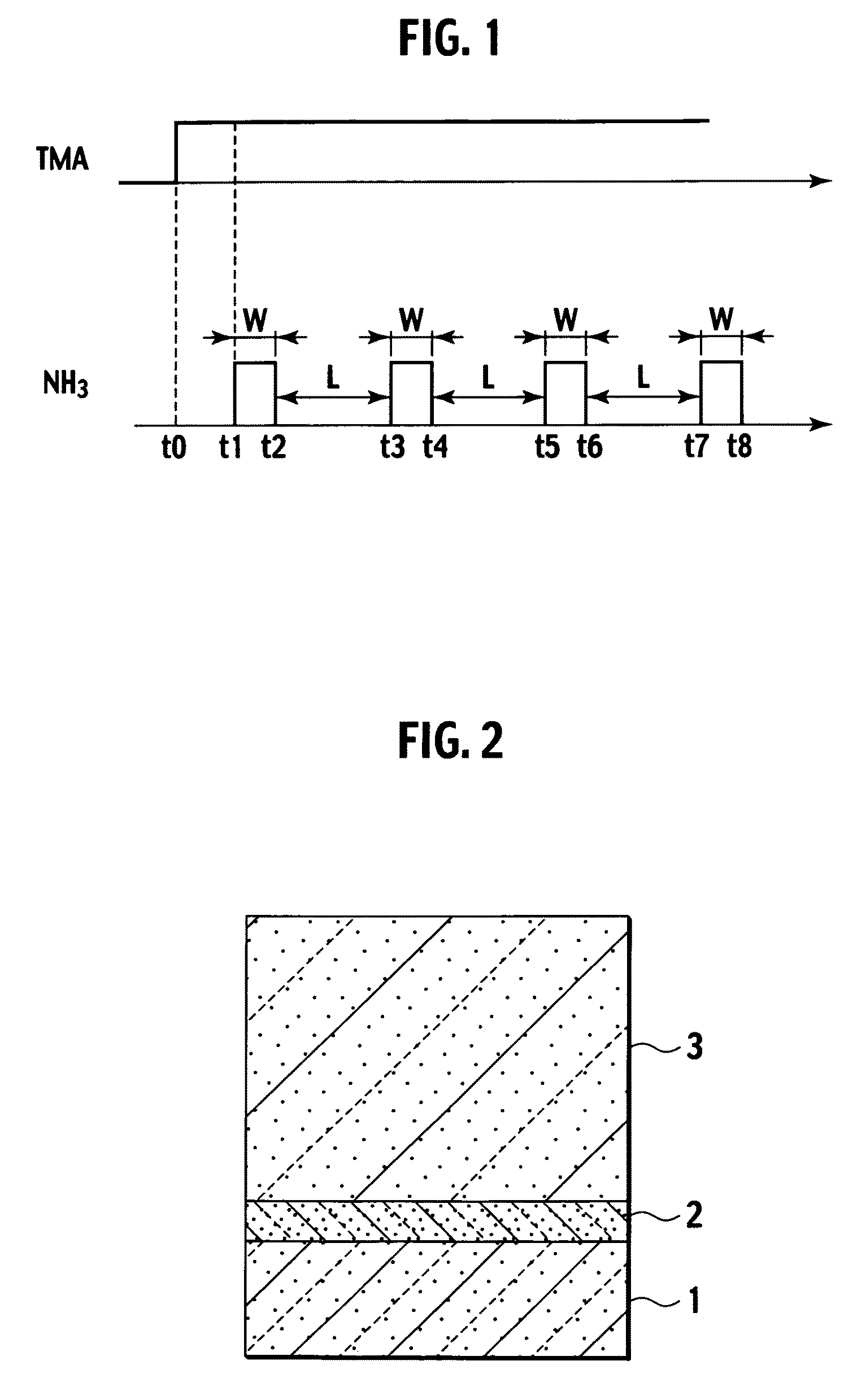
[0059]An embodiment of the present invention will be described below with reference to the drawings. FIG. 1 is a time chart for illustrating principal steps of a method of manufacturing a nitride semiconductor according to the present invention. FIG. 2 illustrates a basic structure of the nitride semiconductor manufactured according to the manufacturing method of the present invention.

[0060]An AlN buffer layer 2 is formed on top of a sapphire substrate 1 that serves as a growth substrate, and then a nitride semiconductor crystal 3 is grown on top of the AlN buffer layer 2. This nitride semiconductor is formed by a known method, such as the MOCVD method. Note that the nitride semiconductor crystal 3 represents a quaternary mixed crystal of AlGaInN, what is commonly known as a group III-V nitride semiconductor, and can be expressed as AlxGayInzN (x+y+z=1, 0≦x≦1, 0≦y≦1, 0≦z≦1).

[0061]Some of the characteristic features of the present invention are: the high temperature of 900° C. or hig...


PUM


Abstract

The present invention provides a method of manufacturing a nitride semiconductor capable of improving the crystallinity and the surface state of the nitride semiconductor crystal formed on top of a high-temperature AlN buffer layer. An AlN buffer layer is formed on top of a growth substrate, and then nitride semiconductor crystals are grown on top of the AlN buffer layer. In a stage of manufacturing the nitride semiconductor, the crystal of the AlN buffer layer is grown at a high temperature of 900° C. or higher. In addition, an Al-source material of the AlN buffer layer is started to be supplied first to a reaction chamber and continues to be supplied without interruption, and then a N-source material is supplied intermittently.

Description

TECHNICAL FIELD[0001]The present invention relates to a method of manufacturing a nitride semiconductor including an AlN buffer layer, and also relates to a nitride semiconductor element.BACKGROUND ART[0002]A lot of development has been made in semiconductor elements made of gallium nitride compound semiconductors, i.e., group-III-V nitride semiconductors (hereafter referred to as nitride semiconductors). Some of the applications of nitride semiconductors are: blue LEDs used as the light sources for illumination, back light or the like; LEDs used for multicoloration; and LDs. The manufacturing of nitride semiconductor in a form of bulk single crystal is difficult. Accordingly, GaN is grown on top of a substrate of different kinds, such as sapphire and SiC, by utilizing the MOCVD (metal organic chemical vapor deposition) method. The sapphire substrate is excellently stable in a high-temperature ammonia atmosphere in the epitaxial growth process, and is especially used as a growth sub...

Claims


Application Information

Patent Timeline
Patent Type & Authority Patents(United States)
IPC IPC(8): H01L33/06H01L21/00H01L33/12H01L33/32
CPCC30B25/14C30B25/183C30B29/403H01L21/0242H01L21/02458H01L21/0254H01L21/0262H01L33/007H01L33/10H01L33/12
Inventor SHAKUDA, YUKIO
Owner ROHM CO LTD
Why Eureka
Try Eureka