Light emitting device and electronic device
a technology of light emitting devices and electronic devices, which is applied in the direction of thermoelectric devices, discharge tubes/lamp details, discharge tubes luminescnet screens, etc., can solve the problems of small voltage and luminance efficiency reduction, low productivity, and low number of processes, so as to reduce voltage and luminance efficiency, improve color purity, and reduce power consumption
- Summary
- Abstract
- Description
- Claims
- Application Information
AI Technical Summary
Benefits of technology
Problems solved by technology
Method used
Image
Examples
embodiment mode 1
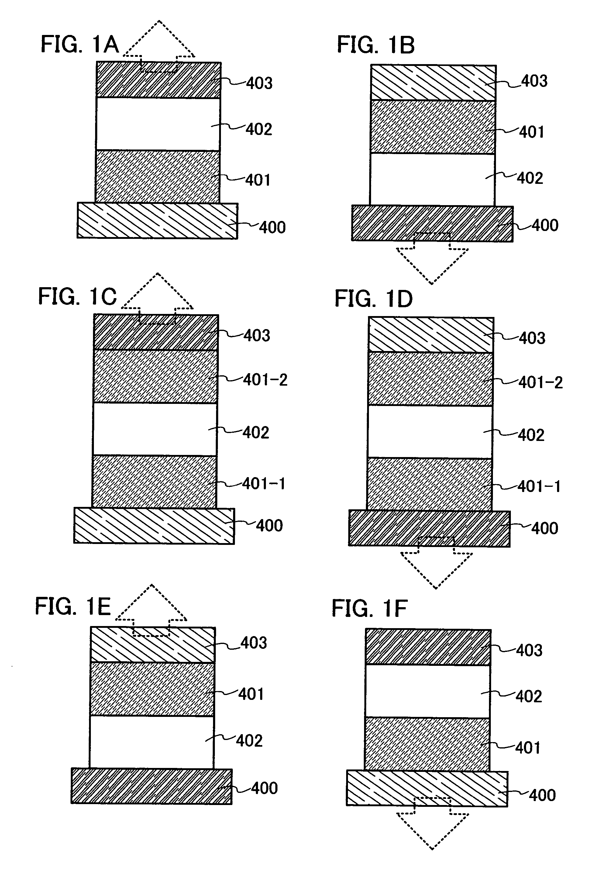
[0037]FIG. 1A is a frame format showing one mode of a light emitting element of the present invention. In a light emitting element of the present invention in FIG. 1A, a layer including an organic compound formed by a buffer layer 401 and a light emitting laminated body 402 is sandwiched between a pair of electrodes composed of a first electrode 400 and a second electrode 403 over an insulator which is not shown. In FIG. 1A, a structure in which light is extracted from a second electrode 403 side will be explained.
[0038]Although the first electrode 400 may be formed to have a single layer or a multilayer, the first electrode 400 is formed to be an electrode having high reflectance. Although the second electrode 403 may be formed to have a single layer or a multilayer, the second electrode 403 is formed as a translucent electrode with respect to light emitted from the light emitting element. According to the light emitting element of the present invention, light emission can be obtai...
embodiment mode 2
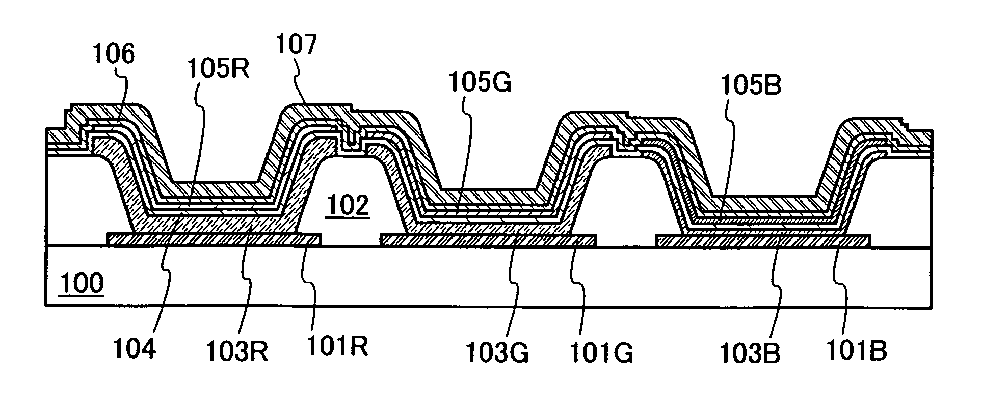
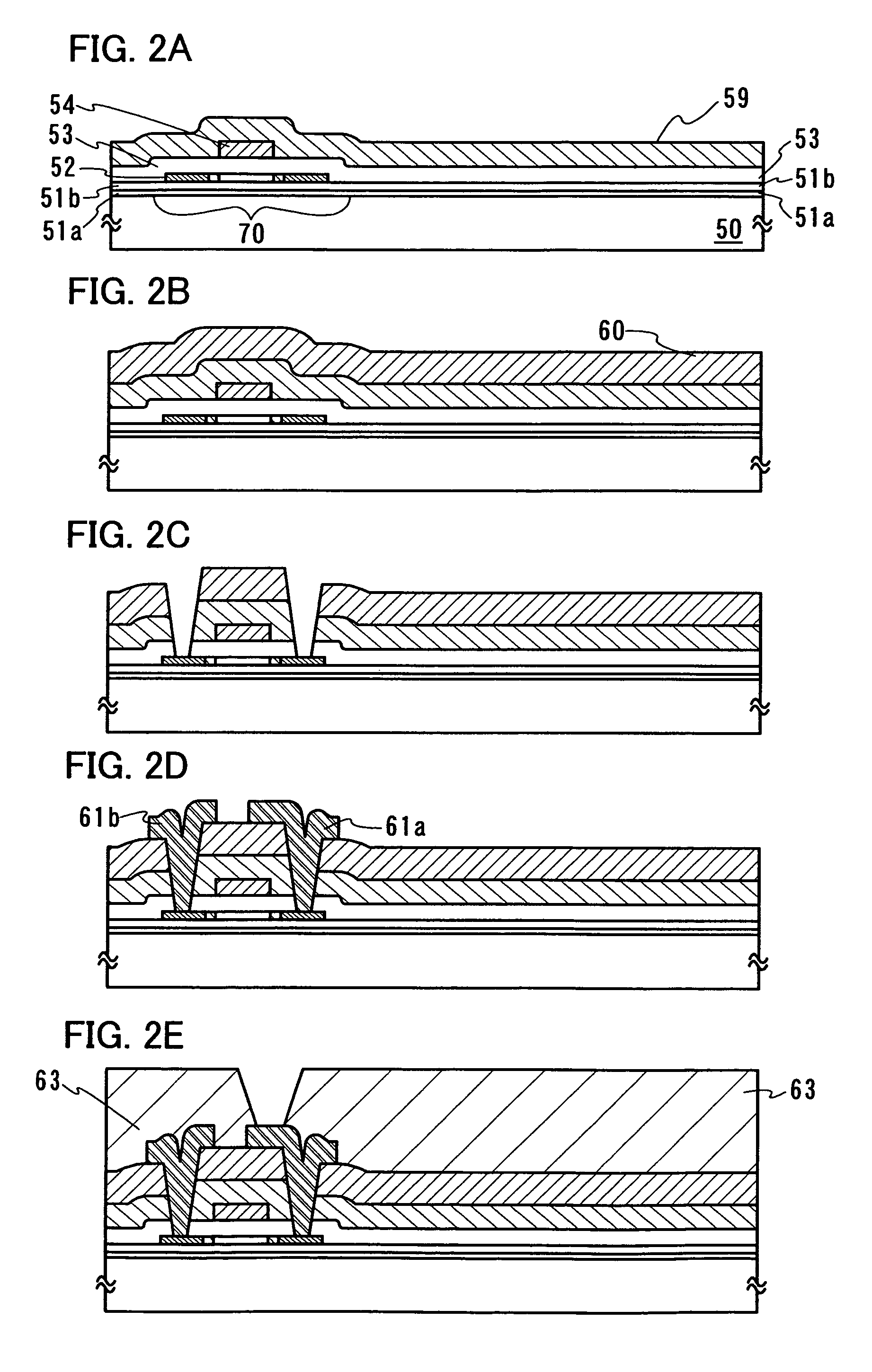
[0175]In this embodiment mode, a manufacturing method of a light emitting device of the present invention will be explained with reference to FIGS. 2A to 2E, FIGS. 3A to 3C, and FIG. 4. It is to be noted that an example of manufacturing an active matrix light emitting device in which light is emitted to a second electrode side is shown in this embodiment mode. In a case of full color display using light emitting elements each having a different wavelength, the arrangement of a pixel of each color is not particularly limited, and desired arrangement such as stripe arrangement or delta arrangement can be applied. In particular, the delta arrangement in which each of the pixels are arranged in a delta array can be preferably applied in a case of using a light emitting element exhibiting three types of luminescent color such as red, green, and blue. The pixel of the delta arrangement is ideal for a light emitting device which displays an image such as a television.
[0176]As a matter of c...
embodiment mode 3
[0214]In this embodiment mode, an outer appearance of a panel of an active matrix light emitting device, which is a display device of the present invention, will be described with reference to FIGS. 5A and 5B. FIG. 5A is a top view of a panel in which a transistor and a light emitting element formed over a substrate are sealed with a sealing material that is formed between the substrate and a counter substrate 4006. FIG. 5B is a cross-sectional view of FIG. 5A. The light emitting element of this panel has a structure as shown in Embodiment Mode 1.
[0215]A sealing material 4005 is provided so as to surround a pixel portion 4002, a signal line driver circuit 4003, and a scanning line driver circuit 4004 that are provided over a substrate 4001. The counter substrate 4006 is provided over the pixel portion 4002, the signal line driver circuit 4003, and the scanning line driver circuit 4004. Thus, the pixel portion 4002, the signal line driver circuit 4003, and the scanning line driver ci...
PUM
 Abstract
Description
Claims
Application Information


