Embedded electronic device package structure

a technology of electronic devices and package structures, applied in the direction of cross-talk/noise/interference reduction, printed circuit aspects, printed circuit non-printed electric components association, etc., can solve the problems of increasing the size of the device, increasing the complexity increasing the property issue of the semiconductor device, so as to reduce the volume of the package, simplify the manufacturing process, and extend the effect of electromagnetic shielding

Active Publication Date: 2014-05-27
UNIMICRON TECH CORP
View PDF7 Cites 38 Cited by
  • Summary
  • Abstract
  • Description
  • Claims
  • Application Information

AI Technical Summary

Benefits of technology

[0017]Based on the description above, in the embedded electronic device package structure of the present invention, the electronic device is disposed in the cavity penetrating through the core layer, and the inner surface of the cavity are covered with a shielding metal layer. Also, the conductive vias are configured to connect the shielding metal layer to the outer surfaces of the first dielectric layer and the second dielectric layer. Accordingly, the shielding metal layer connected to the conductive vias not only may be the path of electrical connection, but also provide the electronic device with the function of ele

Problems solved by technology

The complication of semiconductor devices has been increased, and at least part of the reasons is due to user's demands for increasing processing speed and decreasing the sizes of the devices.
Although the advantages of increasing processing speed and decreasing sizes of the devices are significant, it also causes property issue of the semiconductor device.
Semiconductor devices with smaller size suffer from EMI issue more seriously, because the semiconductor devices (with smaller sizes) are disposed in an electronic system with higher density, such that the neighboring semiconductor devices receive stronger and unwanted electromagnetic emission.
However, even though the conductive casing may diminish the electromagnetic interference, there are a lot of disadvantages in using t

Method used


Image

  • Embedded electronic device package structure
  • Embedded electronic device package structure

Examples


Embodiment Construction

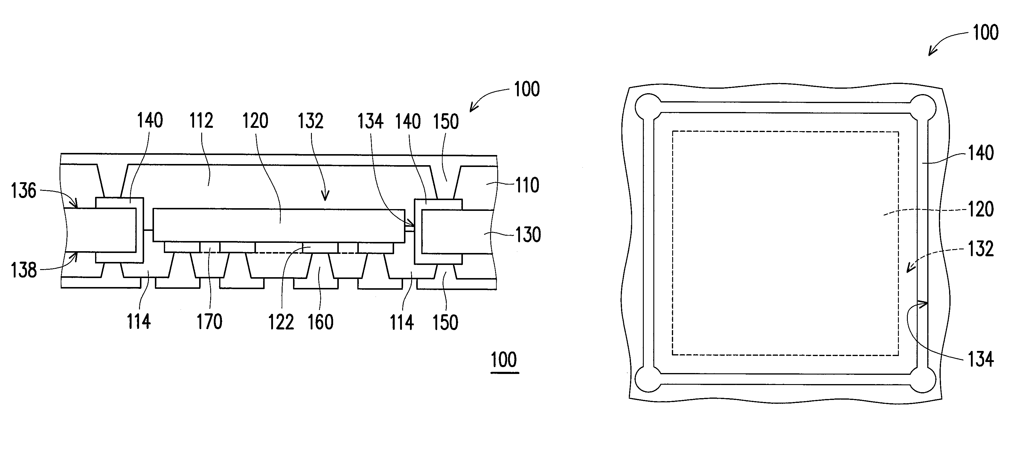
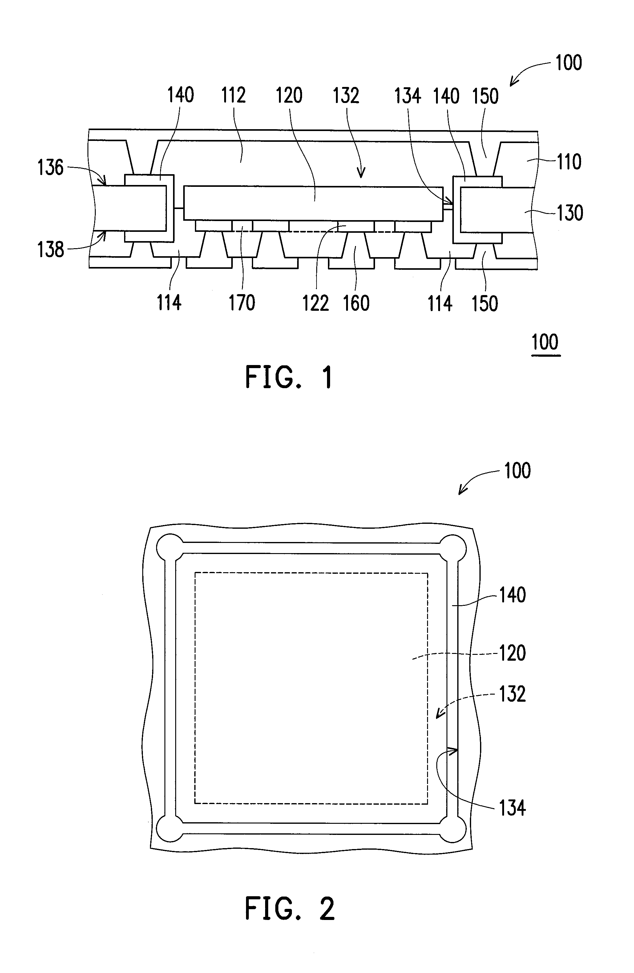
[0022]FIG. 1 is a schematic cross-sectional view of an embedded electronic device package structure according to an embodiment of the present invention. FIG. 2 is a schematic top view of the embedded electronic device package structure in FIG. 1. Referring to both FIG. 1 and FIG. 2, in the present embodiment, the embedded electronic device package structure 100 includes a core layer 130, an electronic device 120, a first dielectric layer 112, a second dielectric layer 114, a shielding metal layer 140 and a plurality of first conductive vias 150. The core layer 130 includes a first surface 136, a second surface 138 opposite to the first surface 136 and a cavity 132. The electronic device 120 is disposed in the cavity 132. The cavity 132 penetrates through the core layer 130. The method of forming the cavity 132 is, for example, laser drilling, but the present invention is not limited thereto.

[0023]To be specific, the embedded electronic device package structure 100 further includes a...


PUM


Abstract

An embedded-electronic-device package includes a core layer, an electronic device, a first dielectric layer, a second dielectric layer, a shielding-metal layer and conductive vias. The core layer includes a first surface, a second surface opposite to the second surface and a cavity penetrating the core layer. The electronic device is disposed in the cavity including an inner surface. The first dielectric layer disposed on the first surface is filled in part of the cavity and covers part of the electronic device. The second dielectric layer disposed on the second surface is filled in rest of the cavity, covers rest of the electronic device. The first and second dielectric layers cover the electronic device. The shielding-metal layer covers the inner surface. The conductive vias are respectively disposed in the first and second dielectric layers and extended respectively from outer surfaces of the first and second dielectric layers to the shielding-metal layer.

Description

BACKGROUND OF THE INVENTION[0001]1. Field of the Invention[0002]The present invention relates to a package structure, in particular, to an embedded electronic device package structure.[0003]2. Description of Related Art[0004]The complication of semiconductor devices has been increased, and at least part of the reasons is due to user's demands for increasing processing speed and decreasing the sizes of the devices. Although the advantages of increasing processing speed and decreasing sizes of the devices are significant, it also causes property issue of the semiconductor device. In particular, higher clock speed may increase the frequency of converting signal level, such that the electromagnetic emission with higher frequency or shorter wavelength is increased. Electromagnetic emission can be radiated out from a source semiconductor device and emitted into a neighboring semiconductor device. If the electromagnetic emission emitting toward the neighboring semiconductor device is stron...

Claims


Application Information

Patent Timeline
IPC IPC(8): H01L23/60
CPCH01L24/19H01L2924/0002H01L23/60H01L23/552H05K1/0218H05K1/185H05K3/4602H05K2201/0715H01L2224/04105H01L2924/3025
Inventor CHUO, YU-CHENCHENG, WEI-MING
Owner UNIMICRON TECH CORP
Why Eureka
Try Eureka