Resin composition and semiconductor device produced using resin composition

a technology of resin composition and semiconductor devices, applied in the direction of semiconductor/solid-state device details, coatings, organic non-macromolecular adhesives, etc., can solve the problems of no junction formation, detachment cracking, and warpage of reflowing, and achieve excellent interfacial adhesion, reduce the effect of reflowing and warpag

Inactive Publication Date: 2014-06-17
SUMITOMO BAKELITE CO LTD
View PDF11 Cites 2 Cited by
  • Summary
  • Abstract
  • Description
  • Claims
  • Application Information

AI Technical Summary

Benefits of technology

[0027]The resin compositions of the present invention are capable of imparting superior reliability to semiconductor devices, in that they result in small warpage of the semiconductor devices, excellent interfacial adhesion, and no occurrence of failures, such as detachment and cracks, also under circumstances at high temperatures of 220° C. or higher.

Problems solved by technology

Area mounting semiconductor devices are thinner, as compared to conventional packages in which each surface of a substrate is subjected to encapsulation, and thus tend to have a greater warpage resulting from differences in coefficient of thermal expansion between component materials, and often suffer a problem that causes detachment and cracking to occur during reflowing.
), there has become more apparent a problem that no junctions are formed due to warpage of the package during mounting of electronic devices as described above.
Furthermore, a reflow process at high temperatures will increase internal stress of a package, and thus will be prone to cause detachment and eventually cracks in the inside of a semiconductor product during the reflow process.
However, the smoothness of the nickel-palladium plating itself and the presence of gold result in reduced adhesion force, as compared with usual silver-plated copper frames and others.
Reduction of adhesion force will cause detachment and cracks in the inside of a semiconductor product during reflowing.
By using only these methods, however, sufficient solutions cannot be provided for failures that are caused in the above-described semiconductor devices.

Method used


Image

  • Resin composition and semiconductor device produced using resin composition
  • Resin composition and semiconductor device produced using resin composition
  • Resin composition and semiconductor device produced using resin composition

Examples


synthesis example 1

Compound A1

Synthesis of n-Pentyl Maleimidoacetate

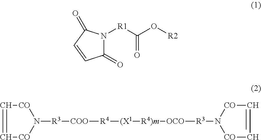
[0069]In a separable flask equipped with a Dean-Stark trap, maleimidoacetic acid (reagent grade) (31.0 g, 0.2 mol), p-toluenesulfonic acid (reagent grade) (5.2 g, 0.03 mol), and toluene (reagent grade) (300 ml) were charged. Then, the mixture was stirred and reacted under reduced pressure at 80° C. for 1 hour with dropwise addition of n-pentanol (reagent grade) (17.6 g, 0.2 mol). After the dropwise addition, the mixture was stirred for another 4 hours for allowing the reaction to be continued. During the reaction, the water formed was removed with the Dean-Stark trap. After the reaction, toluene (300 ml) was added and the mixture was washed three times with ion-exchanged water (100 ml). Then, the organic phase obtained was collected and subjected to removal of the toluene by evaporation using an evaporator and a vacuum dryer to give n-pentyl maleimidoacetate (43.5 g). (Yield: ca. 91%. The absence of maleimidoacetic acid and n-pentanol...

synthesis example 2

Compound A2

Synthesis of 2-Ethylbutyl Maleimidoacetate

[0072]2-Ethylbutyl maleimidoacetate (47.3 g) was obtained in the same manner as in Synthesis Example 1, except that in Synthesis Example 2,2-ethylbutanol (reagent grade) (20.0 g) was used instead of n-pentanol (17.6 g). (Yield: ca. 88%. The absence of maleimidoacetic acid and 2-ethylbutanol was verified by GPC measurement. The presence of 2-ethylbutyl maleimidoacetate was verified by 1H-NMR measurement using DMSO-d6. This compound is referred to hereinafter as Compound A2).

[0073]In Compound A2, R1 is an alkylene group having 1 carbon atom, R2 is a branched alkyl group having 6 carbon atoms, and the sum of carbon atoms of R1 and R2 is 7.

(Material Values of Compound A2)

[0074]1H-NMR (400 MHz, DMSO-d6): 6.9 ppm (2H, —CH═CH—); 4.0 ppm (2H, —CH2—COO—); 3.8 ppm (2H, —O—CH2—)

synthesis example 3

Compound A3

Synthesis of n-Pentyl Maleimidocaproate

[0075]n-Pentyl maleimidocaproate (45.2 g) was obtained in the same manner as in Synthesis Example 1, except that maleimidocaproic acid (reagent grade) (38.6 g) was used instead of maleimidoacetic acid (31.0 g), which was used in Synthesis Example 1. (Yield: ca. 86%. The absence of maleimidocaproic acid and n-pentanol was verified by GPC measurement. The presence of n-pentyl maleimidocaproate was verified by 1H-NMR measurement using DMSO-d6. This compound is referred to hereinafter as Compound A3).

[0076]In Compound A3, R1 is a straight chain alkylene group having 5 carbon atoms, R2 is a straight chain alkyl group having 5 carbon atoms, and the sum of carbon atoms of R1 and R2 is 10.

(Material Values of Compound A3)

[0077]1H-NMR (400 MHz, DMSO-d6): 6.9 ppm (2H, —CH═CH—); 2.3 ppm (2H, —CH2—COO—); 3.7 ppm (2H, —O—CH2—)


PUM

PropertyMeasurementUnit
melting pointaaaaaaaaaa
temperaturesaaaaaaaaaa

Abstract

A resin composition of the present invention includes a maleimide derivative (A) represented by a general formula (1) and a bis-maleimide compound (B) represented by a general formula (2). In the general formula (1), R1 represents a straight chain or branched alkylene group having 1 or more carbon atoms, R2 represents a straight chain or branched alkyl group having 5 or more carbon atoms, and the sum of carbon atoms of R1 and R2 is 10 or less. In the general formula (2), X1 represents —O—, —COO—, or —OCOO—, R3 represents a straight chain or branched alkylene group having 1 to 5 carbon atoms, R4 represents a straight chain or branched alkylene group having 3 to 6 carbon atoms, and m is an integer of 1 or more and 50 or less.

Description

TECHNICAL FIELD[0001]The present invention relates to a resin composition and a semiconductor device produced using the same.[0002]This application claims priority on Japanese Patent Application No. 2010-199889, filed Sep. 7, 2010, the content of which is incorporated herein by reference.BACKGROUND ART[0003]In recent years, higher integration and surface mounting of electronic devices are employed from year to year in market trends toward making electronic equipment smaller, lighter, and highly functioning. For example, making semiconductor devices higher in pin count and thinner is approaching a limit in conventional surface-mounting semiconductor devices, represented by Quad Flat Packages (QFPs) and Small Outline Packages (SOPs), while in order to address need for making them further higher in pin count and thinner, area mounting semiconductor devices such as Lead Frame-Chip Scale Packages (LF-CSPs) and Ball Grid Arrays (BGAs) have been newly developed as next-generation semicondu...

Claims


Application Information

Patent Timeline
Patent Type & Authority Patents(United States)
IPC IPC(8): C08F222/40C08F220/70
CPCH01L23/295C08F222/40H01L2924/12044C09D135/00C08F32/04H01L23/293C09D4/00C09J4/00H01L2924/0002C08F222/402H01L2924/00C08F222/404C08F222/26C08L35/00
Inventor KAWANA, TAKASHIKANAMORI, NAOYAMURAYAMA, RYUICHI
Owner SUMITOMO BAKELITE CO LTD
Why Eureka
Try Eureka